
センターのご紹介
Introduction of the Center
Language
- 日本語
- English
Nanohubとは
What is Nanohub
ポストコロナのデジタル変革を牽引する半導体デバイスシステムの重要性が益々クローズアップされる現在、ナノスケールまで微細化した半導体素子・回路に、センシング、ヘルスケア、量子計算など新たな機能を実現する要素を集積した次世代の機能融合システムをラピッドプロトタイピングできる拠点が今まさに必要とされています。
本センターは、東大内の複数の組織で運営管理していた最先端のナノデバイス製造共用設備と材料要素技術を本センターに統合いたしました。自動化推進によってコロナ禍でも止まらない共同利用拠点を整備し、スピード感のあるベンチャー育成と産学連携等によりデジタル変革を加速いたします。電子デバイス、光デバイス、M/NEMS、微小流体デバイスなどの試作開発環境を整えます。これらのデバイスの設計、製作、評価、および関連する材料・プロセス開発からに回路を含むシステム融合を一気通貫に学べる半導体人材育成の場を提供し、デジタル変革を担う人材養成を行います。
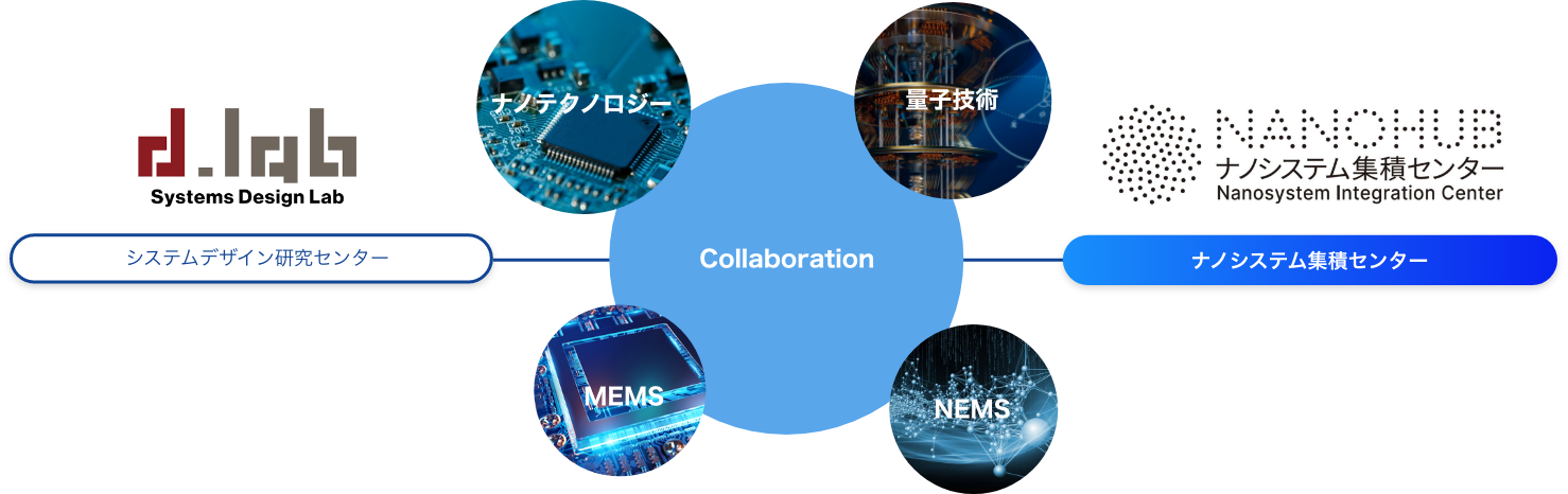
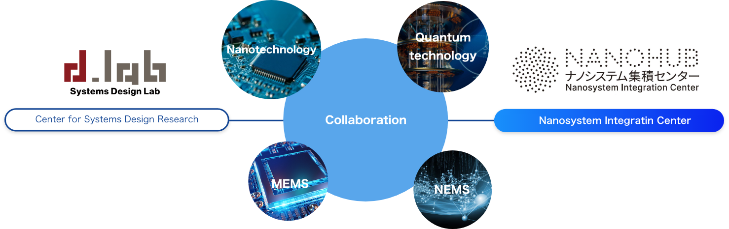
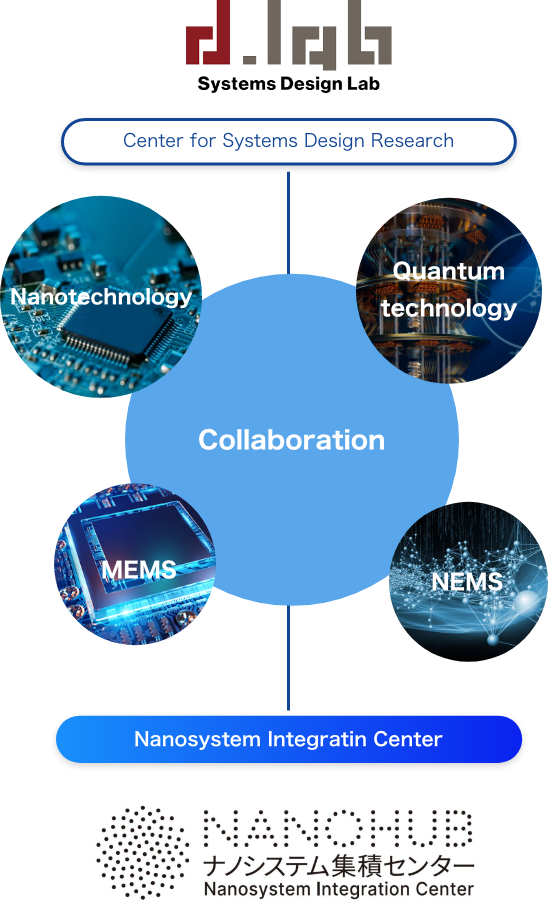
本センターでは、試作したデバイス要素に、それを駆動しサイバー空間に接続するための回路群をシステムデザイン研究センター(d.lab)との協業により組み合わせて実装し、世界最先端の融合システムを迅速に試作することを可能にします。
Now that the importance of semiconductor device systems that drive the post-coronavirus digital transformation is gaining more and more attention, semiconductor elements and circuits that have been miniaturized to the nanoscale are being used to realize new functions such as sensing, healthcare, and quantum computing. There is a real need for a base for rapid prototyping of integrated next-generation functional fusion systems.
This center has integrated cutting-edge shared equipment for nanodevice manufacturing and material element technology, which had been operated and managed by multiple organizations within the University of Tokyo. By promoting automation, we will develop a shared use base that will not stop even during the corona crisis, and accelerate digital transformation through speedy venture development and industry-academia collaboration. We prepare a prototype development environment for electronic devices, optical devices, M/NEMS, microfluidic devices, etc. We will provide a place for semiconductor human resource development where you can learn everything from the design, production, evaluation of these devices, related material / process development, to system integration including circuits, and develop human resources who will be responsible for digital transformation.
At this center, in collaboration with the System Design Research Center (d.lab), we combine and implement prototype device elements with circuits to drive them and connect them to cyberspace, and quickly build the world's most advanced fusion system. It is possible to prototype to
目的
Objective
Society5.0からその先の未来社会には、我々の暮らす物理世界と、情報通信のサイバー世界を仲立ちする 電気機械デバイス・システム「センサ・アクチュエータ」の存在が欠かせません。東京大学では、 武田先端知ビルスーパークリーンルーム( 武田 SCR )を核に、 産学官に開かれた 半導体デバイス 研究のオープンプラットフォーム を整備運用し、規模を拡大してきました。
ナノテクノロジー・量子技術・ MEMS ・ NEMS などの研究領域における優れたインフラとしてのクリーンルームとそこに設置されている多くの装置群をより活用して研究を進展させ、新たな知を生み出すとともに、微細加工装置から分析機器に至るまで東京大学の保有するナノテク関連の研究資源を実質的に集結させ、学内外の先生方のみならず、産業界にも利用していただき、社会に開かれた浅野キャンパスの中心的な存在としてより活性化させることを目的とし、Nanohubは発足いたしました。超微細加工技術と半導体の融合による新展開にご期待ください。
未来社会をデバイスから創りたい方、システムとして実装したい方、幅広い立場の方々のご利用を歓迎いたします。
In the future society beyond Society 5.0, electromechanical devices and systems "sensors and actuators" will be indispensable to mediate between the physical world in which we live and the cyber world of information and communication. The University of Tokyo has established and expanded an open platform for semiconductor device research open to industry, academia, and government, centered on the Takeda SCR (Takeda Advanced Technology Building Super Clean Room).
The clean room is an excellent infrastructure for research in the fields of nanotechnology, quantum technology, MEMS, and NEMS, and the many instruments installed there can be utilized to further develop research and create new knowledge. The Nanohub was established with the aim of bringing together the University of Tokyo's nanotechnology-related research resources, from microfabrication equipment to analytical instruments, and making them available not only to professors inside and outside the University, but also to industry, thereby reinvigorating the Asano campus as a center open to society. We hope you will look forward to new developments through the fusion of ultrafine processing technology and semiconductors.
We welcome people from a wide range of backgrounds who want to create the future society from devices and implement it as a system.
従来との違い、共同研究の推進
Difference from conventional
今までのクリーンルーム(CR)は、共用利用の施設であり、共に装置を利用することはあっても、研究は各々個別で行っていました。そのため、CRユーザー同士では、誰が何の装置を使用しているか把握はしていても、どんな研究をしているのか、研究の中身を知る機会は多くはなかったのではないでしょうか。これからは、Nanohubが出会いの場となり、研究者同志の協力および研究上のつながりの強化を推進します。ユーザー同士、「共同研究」という新たな形で装置だけでなく研究面でもつながり、より発展していくことを目指します。
共同研究は、50年程前から重要な研究方法として考えられてきました。同研究の成功を確実にするためには多種多様なコミュニケーションが必要となりますが、異分野の交流はさまざまな期待を生み出し、研究資金獲得の際も競争上有利となり、より質の高い研究成果が上がり、実用化も加速されるはずです。社会に強いインパクトを与える新しい種類の共同研究は、多くの人が強い関心を持ち注目を集めることになるでしょう。
Until now, clean rooms (CR) have been shared facilities, and even though they used equipment together, research was conducted individually. Therefore, even if CR users knew who was using what equipment, they probably didn't have many opportunities to know what kind of research was being done. From now on, Nanohub will become a meeting place to promote collaboration and strengthen research ties among researchers. We aim to connect users not only with equipment but also with research in a new form of "joint research" and further develop.
Collaborative research has been considered an important research method for some 50 years. Although a wide variety of communication is needed to ensure the success of research, interactions between different disciplines should create different expectations, give a competitive advantage when it comes to obtaining research funding, produce higher quality research results and accelerate practical applications. New types of collaborative research with a strong impact on society will attract strong interest and attention from many people.
Translated with www.DeepL.com/Translator (free version)
他センターとの協業
Collaboration with d.lab
Nanohubは、試作したデバイス要素に、それを駆動しサイバー空間に接続するための回路群をシステムデザイン研究センター(d.lab)との協業により組み合わせて実装し、世界最先端の融合システムを迅速に試作することを可能にします。
2022年7月1日には、武田SCRに集うナノテクノロジーに関する先端知を生かして、更に高度な技術として発展させるための研究を行う拠点として、附属システムデザイン研究センター(d.lab)基盤デバイス研究部門に寄付講座「ナノシステム集積技術の創製」が設立されました。Nanohubと共に相次いで成立した二つの新しい仕組みは、同じ目標に向かって進むものです。
The Nanohub enables rapid prototyping of the world's most advanced fusion systems by combining prototype device elements with circuits to drive them and connect them to cyberspace in collaboration with the System Design Research Center (d.lab).
On July 1, 2022, an endowed chair, "Creation of Nanosystem Integration Technology," was established in the Fundamental Device Research Division of the System Design Research Center (d.lab) as a center for research to further develop advanced technologies by utilizing the advanced knowledge of nanotechnology gathered at the Takeda SCR. The two new research centers established in tandem with Nanohub are both working toward the same goal: to develop advanced nanotechnology by utilizing cutting-edge knowledge in nanotechnology.

ロゴのご紹介
Introduction of the logo
ロゴマークと略称の文字デザインに利用する円を同一個数にして、マークと文字とで同一性を担保することを狙いとしました。
The logo mark and the circles used in the abbreviated letter design are the same in number to ensure the identity of the mark and the letters. The aim was to ensure the identity of the mark and the letters.
工学系研究科の附属施設
Facilities affiliated with the School of Engineering
本センターは、東大内の複数の組織で運営管理していた最先端のナノデバイス製造共用設備と材料要素技術を統合し、2022年4月に発足いたしました。工学系研究科の13の附属施設のうちのひとつです。
This center was launched in April 2022 by integrating cutting-edge shared equipment for nanodevice manufacturing and material element technology that had been operated and managed by multiple organizations within the University of Tokyo. One of the 13 affiliated facilities of the School of Engineering.
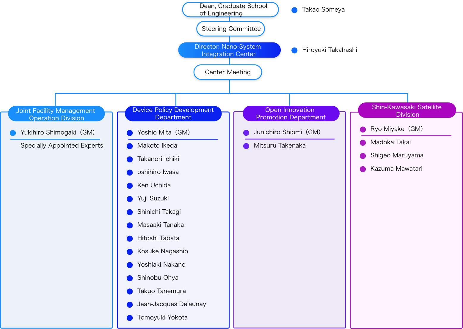
組織構成
Organizational structure
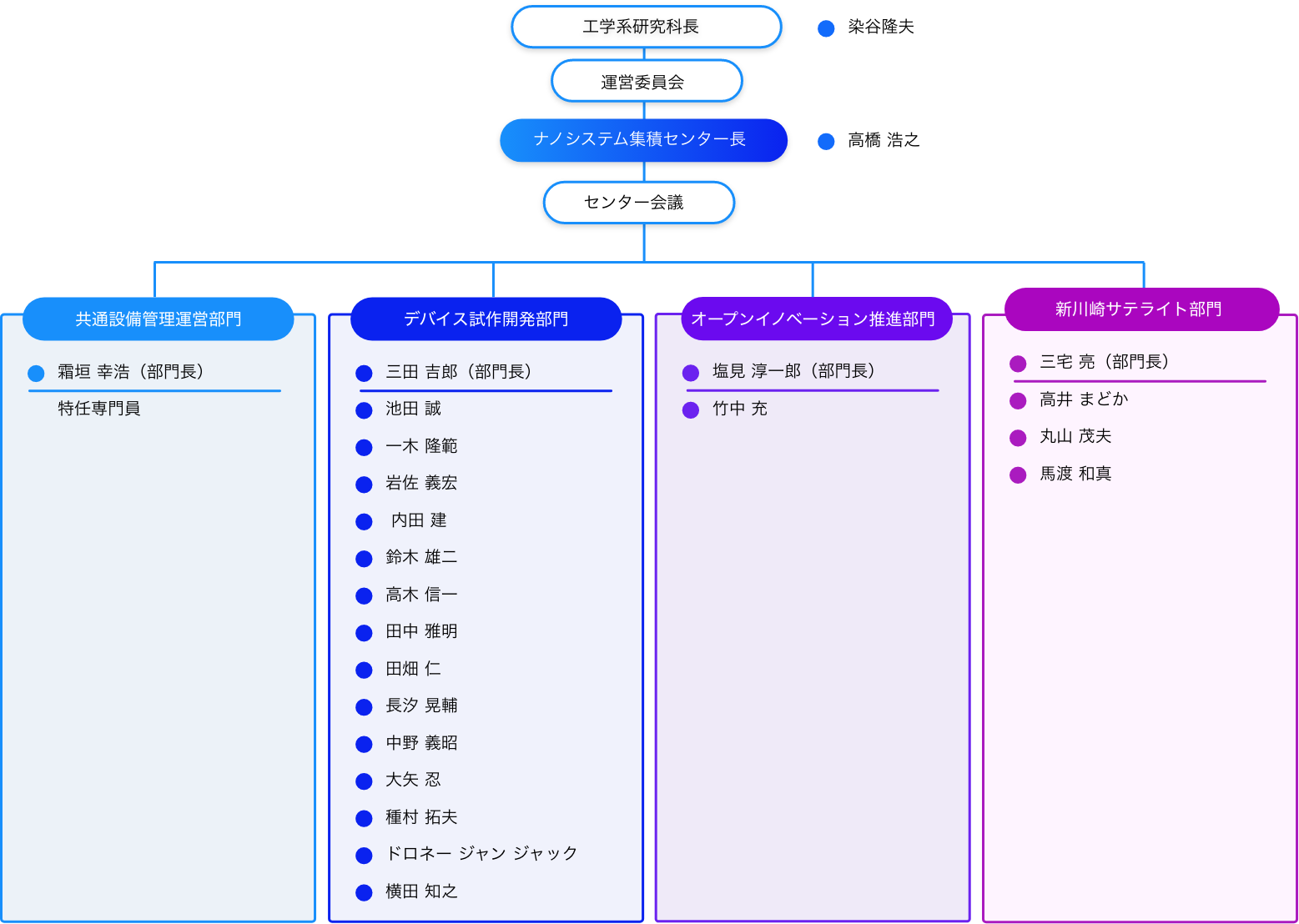
センターは共用設備管理運営部門、デバイス試作開発部門、オープンイノベーション推進部門、新川崎サテライト部門の4つの部門に分かれております。デバイス試作開発部門および新川崎サテライト部門では、共用装置のご利用を提供しております。
The center is divided into four departments: shared equipment management and operation department, device prototype development department, open innovation promotion department, and Shin-Kawasaki satellite department. The Device Prototype Development Department and Shin-Kawasaki Satellite Department offer the use of shared equipment.
デバイス試作開発部門の武田先端知ビルクリーンルーム(浅野キャンパス)では、多様な超微細加工装置が利用できます。新川崎サテライト部門の神奈川県川崎市の新川崎・創造のもり地区には、4大学コンソーシアム(慶応大学、早稲田大学、東京工業大学、東京大学)の下で運営されている共用施設があり、NANOBICオープンラボにて装置が利用できます。
A variety of ultra-fine processing equipment can be used in the Takeda Advanced Science Building Clean Room (Asano Campus) in the Device Prototype Development Division. In the Shin-Kawasaki Sozo no Mori district in Kawasaki City, Kanagawa Prefecture, which is part of the Shin-Kawasaki Satellite Division, there is a shared facility operated by a four-university consortium (Keio University, Waseda University, Tokyo Institute of Technology, and the University of Tokyo). The device is available at


デバイス試作開発部門
Device Prototype Development Department
東京大学浅野キャンパス武田先端知ビルクリーンルームの地下2階にて、多様な超微細加工装置が利用できます。
A variety of ultra-fine processing equipment can be used on the 2nd basement floor of the Takeda Advanced Science Building clean room on the Asano Campus of the University of Tokyo.
新川崎サテライト部門
Shin-Kawasaki Satellite Division
神奈川県川崎市の 新川崎・創造のもり地区に、4大学コンソーシアム(慶応大学、早稲田大学、東京工業大学、東京大学)の下で運営されている共用施設です。
It is a shared facility operated by a four-university consortium (Keio University, Waseda University, Tokyo Institute of Technology, and the University of Tokyo) in the Shin-Kawasaki Sozo no Mori area of Kawasaki City, Kanagawa Prefecture.

