
研究活動の紹介
Introduction of research activities
Language
- 日本語
- English
ナノシステム集積センター
-
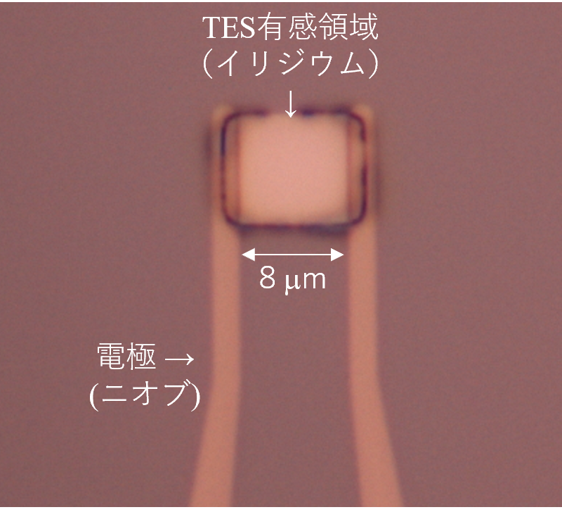 研究室サイトへ To the laboratory site高橋 浩之 研究室 : 量子センシング―量子センサの開発と応用Hiroyuki Takahashi Laboratory : Quantum sensing - Development of quantum sensors and their applicationsさまざまな物理・化学・生物の過程を応用することで、情報を取り出すセンシングは奥が深く、また、境界分野として多くの専門分野をつなぐ部分でもあります。我々は赤外光・X線・ガンマ線・イオンビーム・中性子等の量子放射線を対象として、光電効果・2次電子放出から超伝導相転移・準粒子生成まで電子・イオン・フォノンなどの信号キャリア生成の原理に踏み込んだ高性能センサの開発を行うとともに、コンプトン効果・陽電子消滅・多光子放出過程などの基礎原理を応用するイメージング法の研究、また、専用集積回路の開発など量子センシング研究を学内他部局、国内外の企業や大学・研究所など研究課題に応じ適宜協力しながら進めています。また、計測診断技術にとどまらずに、RI内用療法や中性子捕捉療法などの治療法の研究も行っています。これらの研究は基礎物理・分析から医療応用、非破壊検査、原子力、量子コンピュータにいたる広い範囲にまたがるものを目指しております。Sensing is a profound research field, which relies on many different working principles in various fields, therefore it cultivates an important interdisciplinary area. We are developing new sensors for infrared photons, X-rays, Gamma rays, charged particles, and neutrons using many different working principles such as photoelectric effects, secondary electron emission, superconducting phase transition, quasi-particle formation, etc. We also develop new imaging methods using Compton effects, annihilation of positrons, cascade gamma photon emission, etc. To realize a new sensor system, we need to develop a new application specific integrated circuit as well. We collaborate with many other institutes in Japan or in foreign countries. Application fields include fundamental physics, chemical analysis, non-destructive testing, nuclear engineering, and quantum computing.
共通設備管理運営部門
-
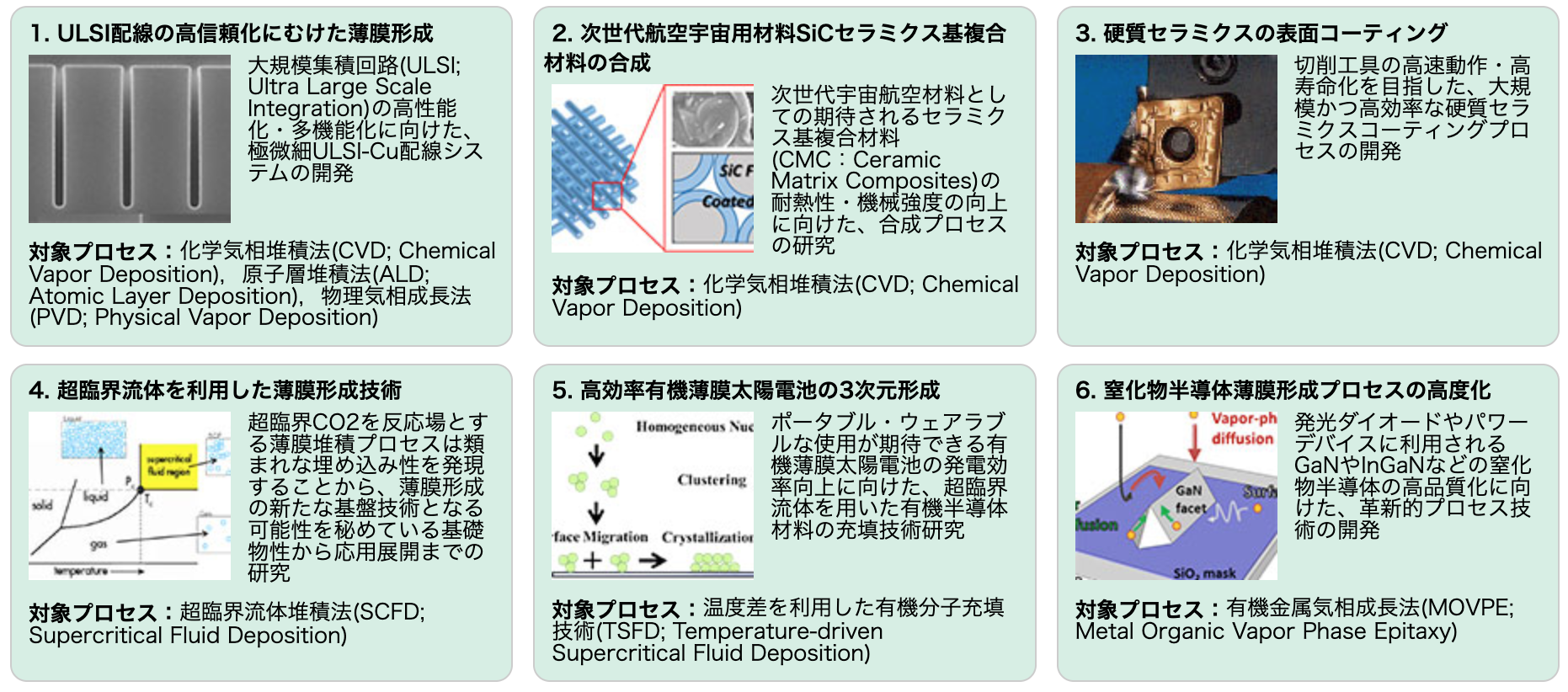 研究室サイトへ To the laboratory site霜垣 幸浩 研究室 : 次世代プロセス技術による機能性材料開発Yukihiro Shimogaki Laboratory : Development of functional materials using next-generation process technologyある空間の中により多くあるいはより高い機能を与えようとしたとき、必然的に構造は複雑化してくる。電子・光デバイスではシリコン等のウェハ表面への微細な3次元構造の形成が求められ、構造材料では繊維強化複合材料や機能性薄膜の表面コートなどが求められるようになってきた。このことは、材料学に基づく機能設計・構造設計に加えて複雑な立体構造の形成技術の開発を示唆している。 そのため我々は、複雑な3次元構造に対し機能性材料を充填あるいは機能性薄膜をコーティングするプロセスにおいて、プロセスの裏側に存在する製膜機構を解析しプロセスが本来持つ性能を最大限引き出す「プロセス設計」、新たな仕組みを導入しプロセス特性を向上させる「プロセス高度化」を行い、材料の機能化、デバイスの高性能化を目指している。When trying to give more or higher functions to a certain space, the structure inevitably becomes more complicated. For electronic and optical devices, the formation of fine three-dimensional structures on the surface of wafers such as silicon is required, and for structural materials, fiber-reinforced composite materials and functional thin film surface coatings are required. This suggests the development of technology for forming complex three-dimensional structures in addition to functional and structural design based on materials science. Therefore, in the process of filling a complex three-dimensional structure with a functional material or coating a functional thin film, we analyze the film formation mechanism that exists behind the process and perform "process design" that maximizes the inherent performance of the process. ”, and ”process sophistication” that introduces new mechanisms and improves process characteristics, aiming for functionalization of materials and high performance of devices.
デバイス試作開発部門
-
 研究室サイトへ To the laboratory site三田 吉郎 研究室 : 知的集積化微小電気機械素子システムの研究Yoshio Mita Laboratory : Intelligent Semicconductor Microdevices Research三田研究室は、知的な集積化微小電気機械素子システムの研究室(iSML)です。半導体プロセス工学、電子デバイス工学、電子回路工学、集積回路工学の学問的裏付のもと、大規模集積回路(VLSI)とMEMSの融合による新たな価値創造に取り組みます。Society5.0、その先の情報技術を担う電子情報機器システム、特に微小電気機械デバイスと集積回路技術を高度化した、社会実装可能な融合システムの研究を数多く実行しています。「不可能」と思えた多くの課題が三田研によって可能になりました。武田先端知ビルスーパークリーンルームでの装置共用事業の中核運営研究室でもあります。Intelligent Semicconductor Microdevices Laboratory (iSML, a.k.a. Mita group) aims at new value creation by integration of VLSI circuits and MEMS devices. The group stands on multi-disciplines such as semiconductor process engineering, electron device engineering, electronics circuit engineering, and integrated circuits engineering. The group is conducting many research topics for electro information devices that will be used in Society 5.0 and beyond. Most of the developed devices can be readily deployed in society, because of the group’s unique integration VLSI-MEMS integration technology. Indeed, many problems that was thought to be impossible has been solved by the group. The group is also the core executive team of Takeda Cleanroom facility operations.
 -
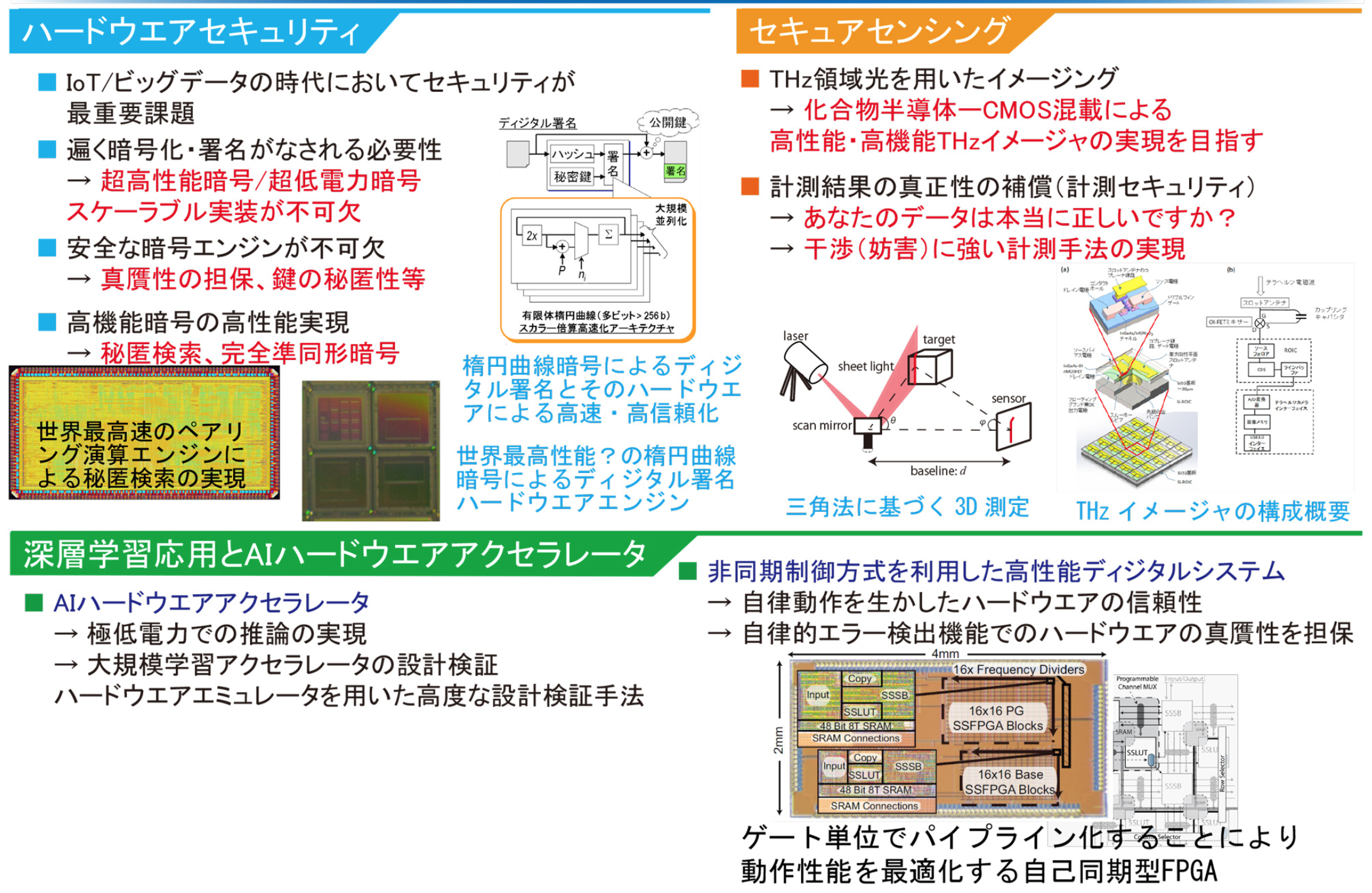 研究室サイトへ To the laboratory site池田 誠 研究室 : ハードウェアセキュリティと計測セキュリティMakoto Ikeda Laboratory : Hardware security and instrumentation securityハードウエアとセキュリティを中心に据えた研究をしています。最先端のプロセスを使用したディジタル・アナログ回路の設計をしており、自ら回路を提案、試作、測定をすることが可能です。自己同期回路、イメージセンサ、Signal Integrity、アナログ技術、RF、CADを大きなテーマとして掲げ、研究を行なっています。My research focuses on hardware and security. We design digital and analog circuits using state-of-the-art processes, and are able to propose, prototype, and measure circuits ourselves. We are conducting research on self-synchronous circuits, image sensors, signal integrity, analog technology, RF, and CAD as major themes.
 -
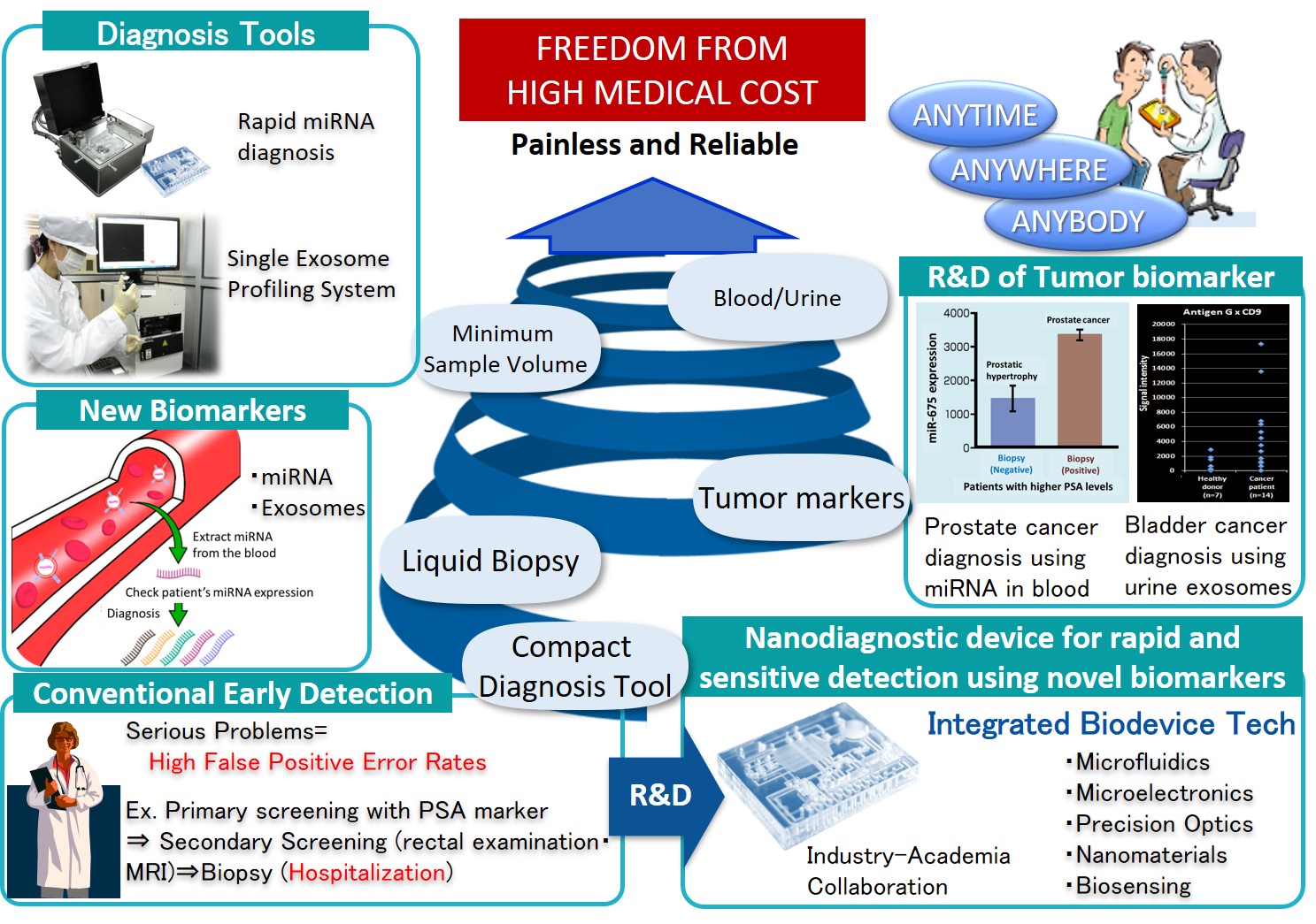 研究室サイトへ To the laboratory site一木 隆範 研究室 : 微細加工技術とナノバイオデバイスの研究開発Takanori Ichiki Laboratory : Research and development of microfabrication technologies and nano-biodevicesULSI製造のための極微細加工プロセスを中心とするプラズマプロセスやMEMS加工の研究から、当該技術のナノバイオテクノロジー、医療分野への応用研究へと展開し、化学や分子生物学、医学等との学際研究領域であるバイオデバイスの分野において、基盤要素技術から実用的なシステム創製に至るまでを研究している。 現在は、がん診断や感染症検査を迅速化するPOCT検査装置、新たな再生医療用材料として注目されるエクソソームの分析·精製ツールの開発、創薬に役立つ高効率スクリーニング用プロテインアレイチップの開発等を通じて新しい診断・治療技術の創出に取り組んでいる。Our research has expanded from research on plasma processes, focusing on ultrafine fabrication processes for ULSI production, to research on the application of these technologies to the fields of nanobiotechnology and nanomedicine, and has developed from basic elemental technologies to the creation of practical systems in the field of biodevices, an interdisciplinary research area with chemistry, molecular biology, medicine, and other fields. His research ranges from basic elemental technologies to the creation of practical systems and devices. Presently, we are working on the creation of new diagnostic and therapeutic technologies through the development of Point-of-Care-Testing devices for rapid cancer diagnosis and infectious disease testing, analysis and purification tools for exosomes, which are attracting attention as a new material for regenerative medicine, and protein array chips for highly efficient screening useful for drug discovery.
 -
 研究室サイトへ To the laboratory site岩佐 義宏 研究室 : イオン運動・配列制御による電子機能学理「イオントロニクス」を創成Yoshihiro Iwasa Laboratory : Creation of electronic functional theory "Iontronics" by controlling ion motion and arrangement現実世界のデバイスは、ほとんどすべて界面を用いてその機能が発現します。半導体デバイスはその顕著な例ですが、単結晶や薄膜単体では実現不可能、あるいは困難な物性・機能を、二次元物質やナノチューブなどを用いて界面・デバイスによって実現することを本研究室は目指しています。 最近では、電気化学と半導体電子工学、さらには物性物理の融合学理に基づく電気二重層トランジスタを提唱・開発し、電界誘起超伝導をはじめとする電子相制御など従来の固体デバイスでは実現不可能な物性・機能を実現してきました。こうした研究をますます発展させ、イオン運動・配列制御による電子機能学理「イオントロニクス」を創成することが本研究室の目的です。Almost all devices in the real world express their functions using interfaces. Semiconductor devices are a prominent example of this, but our laboratory aims to realize physical properties and functions that are impossible or difficult to achieve with single crystals or thin films by interfaces and devices using two-dimensional materials and nanotubes. I'm here. Recently, he has proposed and developed an electric double-layer transistor based on the combined theory of electrochemistry, semiconductor electronics, and condensed matter physics. We have realized physical properties and functions. The purpose of this laboratory is to develop such research more and more and to create electronic functional theory "Iontronics" by controlling ion motion and arrangement.
 -
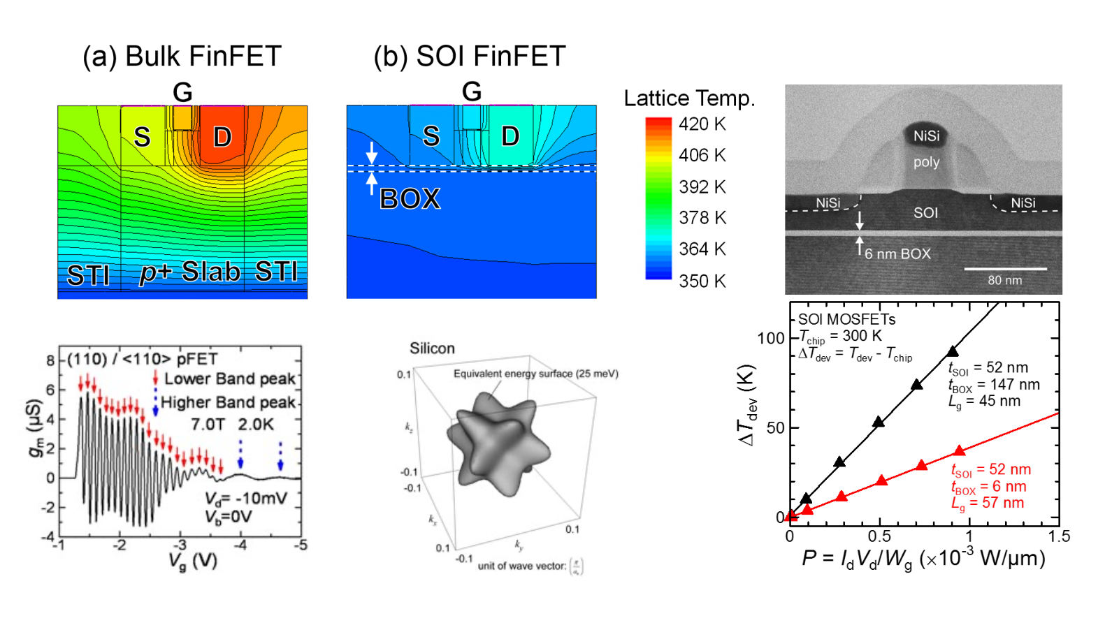 研究室サイトへ To the laboratory site内田 建 研究室 : ナノスケール電子材料を用いたエレクトロニクス・デバイスKen Uchida Laboratory : Electronic devices using nanoscale electronic materials小型・低電力のセンサとコンピューティング・デバイスの研究開発を行っています。私たちの周りを漂う揮発性有機化合物(VolatileOrganic Compounds:VOC)などの「低分子を低エネルギー消費かつ高感度で計測する分子センサ(MolecularSensors)」の研究に力を入れています。分子センサは匂い・香りの計測、工場のプロセスモニタリング、健康状態管理(ヘルス・モニタリング)、スマート農業など、幅広い分野への応用が期待されています。デバイス・レベルでは、分子センサ(ガスセンサ)、CMOSデバイス(シリコン、その他高移動度半導体材料)、ナノシートデバイス(グラフェン、半導体ナノシート)、量子効果デバイスをキーワードとした研究を進めています。We are researching and developing small, low-power sensors and computing devices. We are focusing on research on "Molecular Sensors that measure small molecules with low energy consumption and high sensitivity" such as Volatile Organic Compounds (VOC) floating around us. Molecular sensors are expected to be applied to a wide range of fields, such as odor measurement, factory process monitoring, health monitoring, and smart agriculture. At the device level, our research is focused on molecular sensors (gas sensors), CMOS devices (silicon and other high-mobility semiconductor materials), nanosheet devices (graphene, semiconductor nanosheets), and quantum effect devices.
 -
 研究室サイトへ To the laboratory site鈴木 雄二 研究室 : ウエアラブルデバイスのための高出力エレクトレット環境発電の創成Yuji Suzuki Laboratory : Creation of High-output-power Elecret-based Energy Harvesting for Wearable Devicesエレクトレットは電荷を半永久的に保持させた誘電体であり、エレクトレットを用いた静電誘導発電は、特に小スケール、低周波数の環境振動発電において優れた特性を持つ。本研究では、アモルファスフッ素樹脂をベース材料として量子化学計算と機械学習に基づく革新的エレクトレット材料の開発、ウエアラブルデバイスのための手首装着型回転型エレクトレット発電器の開発、人の歩行時の腕振りモデルの構築と発電器構造の最適化、一部IC化した非線形電源管理回路の開発などを進めている。Electret is a dielectric that retains electric charge semi-permanently, and electrostatic induction power generation using electret has excellent characteristics especially in small-scale, low-frequency vibration energy harvesting. In this study, we are developing an innovative electret material based on amorphous fluorinated polymer as a base material with the aid of quantum chemical analysis and machine learning, and developing a wrist-worn rotational electret generator for wearable devices. We are also working for an arm-swing model for human walking toward optimum design of the generator structure, and the development of an IC-based non-linear power management circuit.
 -
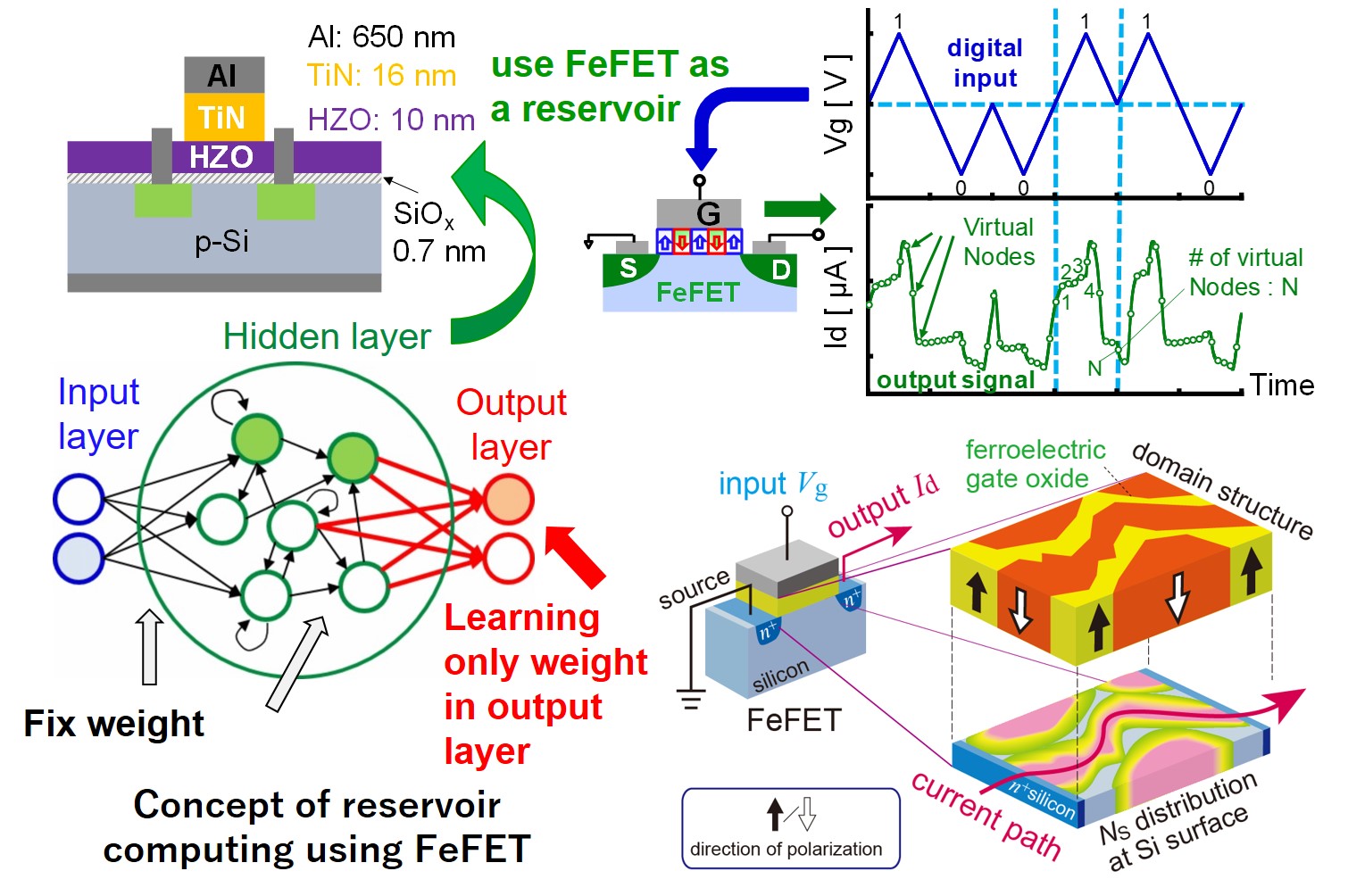 研究室サイトへ To the laboratory site高木 信一 研究室 : 強誘電体デバイスを用いたリザバーコンピューティングShinichi Takagi Laboratory : Reservoir computing using ferroelectric devices計算負荷の軽いAI計算手法として、リザバーコンピューティングが近年注目を集めている。当研究室では、メモリ・イン・ロジック機能や非線形アナログ計算機能をもつ強誘電体ゲートMOSFET(FeFET)やMFMキャパシタが、リザバーコンピューティングを物理実装できるハードウェアとして有望であることを提案し、そのリザバーコンピューティング動作を世界で初めて実証している。強誘電体デバイスを用いたこのリザバーを用いて、極低消費電力で推論・学習を行うことができる新しいAIハードウェアをSiプラットフォーム上に実現する研究を行っている。Reservoir computing has recently attracted attention as an AI computation method with computational load for learning. We have recently proposed that ferroelectric gate MOSFETs (FeFETs) and MFM capacitors with memory-in-logic and nonlinear analog computing functions are promising hardware for the physical implementation of reservoir computing. Also, we have demonstrated its reservoir computing operation for the first time in the world. Using these reservoirs based on ferroelectric devices, we are conducting research to realize new AI hardware on Si platforms that can perform inference and learning with extremely low power consumption.
 -
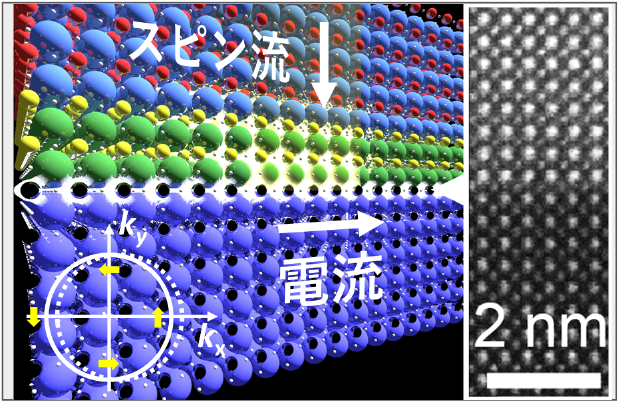
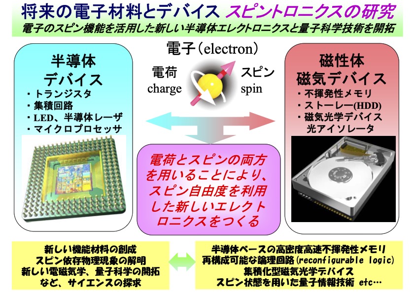 研究室サイトへ To the laboratory site田中 雅明 研究室 : スピントロニクスと量子科学技術による半導体エレクトロニクスの革新Masaaki Tanaka Laboratory : Innovations in Semiconductor Electronics through Spintronics and Quantum Science and Technology電子・スピン物性とデバイス工学を中心にマテリアルサイエンス・物性物理学・デバイス・量子情報科学など、ScienceとTechnologyの広い領域を横断する新分野を開拓し、その知見による半導体エレクトロニクスの革新を目指しています。具体的には、異種物質から成るヘテロ構造・混晶・ハイブリッド構造・ナノ構造など、自然界に存在しない新物質や新構造の形成、それらの光/電子/磁気(スピン)物性の探索と制御、デバイス応用、半導体と磁性(または強磁性体)の融合とそのエレクトロニクスへの応用、スピン自由度を生かした機能材料とデバイス、「スピントロニクス」の開拓研究、トポロジカル物質を含む量子物質の作製、電子の波動関数とスピン、スピン軌道相互作用も含めた量子状態の制御、量子情報デバイスへの応用、量子科学技術の開拓を行っています。We aim to innovate semiconductor electronics by developing new fields that cross a broad spectrum of science and technology, such as materials science, condensed matter physics, device engineering, and quantum information science. Our research includes the formation of new materials and structures that do not exist in nature, such as artificial heterostructures, alloys, hybrid structures, and nanostructures composed of different materials, as well as the exploration of their optical, electronic, and magnetic (spin-related) properties, and device applications. Especially, we study the fusion of semiconductors and magnetism (or ferromagnetism), and the development of functional materials and devices utilizing spin degrees of freedom, exploration of "spintronics". We also explore quantum materials including topological materials, control of quantum states such as electron's wavefunction, spin and spin-orbit coupling, and application to quantum information devices.
 -
 研究室サイトへ To the laboratory site田畑 仁 研究室 : 生体機能に学ぶ革新的省電力、超高感度デバイス研究Hitoshi Tabata Laboratory : Research on Innovative Power-saving Devices and Ultra-sensitive Devices Learning from Biological Function.従来のノイマン型コンピュータの限界が近づく中、Beyond AI、6G以降を支える超消費電力・超並列計算を実現する新しい発想の脳模倣型コンピュータの鍵を握るデバイス研究を実施。特に情報伝達・処理に電子の輸送を伴わない(ジュール熱損の無い)、角運動量伝搬を活用するスピン波(マグノン)デバイスを研究。また脳での情報処理の数学的表現であるハミルトニアンと、スピン”ゆらぎ”物性のスピングラスのそれが同じ表式であることに着目したスピンゆらぎデバイスによるブレイン/ニューロモルフィック、リザバーコンピューティング研究を実施。さらに強誘電体/圧電体薄膜による超低電力駆動弾性波(フォノン)誘起によるマグノニクスデバイス研究を併せて実施。As conventional Neumann-type computers approach their limits, we are researching devices that hold the key to a new concept of brain-mimicking computers that will realize the ultra-low-power consumption and massively parallel computing that will support Beyond AI and 6G and beyond. In particular, he studies spin-wave (magnon) devices that do not involve electron transport (no Joule heat loss) and utilize angular momentum propagation for information transfer and processing. We are also researching brainmorphic and reservoir computing using spin fluctuation devices, caused by the fact that the mathematical expression of information processing in the brain, the Hamiltonian formula, is the same as that of s spin glass, which is a physical property of spin "fluctuation. In addition, we are also conducting research on magnonics devices operated using ultra-low power-driven elastic wave (phonon) by the spin wave-piezoelectric surface acoustic wave combination.
 -
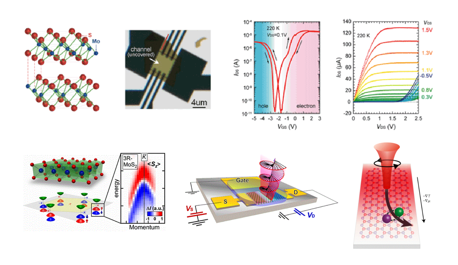
 研究室サイトへ To the laboratory site長汐 晃輔 研究室 : 2次元材料をベースとしたデバイス展開Kosuke Nagashio Laboratory : Device application based on 2 dimensional materialsグラフェン、h-BN、遷移金属ダイカルコゲナイド(TMDC)等の二次元物質の電子デバイス化に取り組んでいる、代表的な成果として、グラフェン/金属界面でのコンタクト抵抗がグラフェンの状態密度で律速されていることの実証 、二次元絶縁体h-BNがダイアモンドを超える絶縁破壊電界を有する起源の解明、二層グラフェンの垂直電界印加によるバンドギャップ形成、MoS2トランジスタにおける界面準位計測及びその低減などが挙げられる、最近では、二次元層状SnSにおいて単層厚さでの強誘電特性を室温で実証しており、空間反転対称性の敗れた結晶における光起電力発電への展開を進めている。We are working on the device application of two-dimensional materials such as graphene, h-BN, and transition metal dichalcogenides (TMDC). Typical achievements are as follows. (i) the contact resistance at the graphene/metal interface is controlled by the small density of states in graphene. (ii) the understanding of the origin for dielectric breakdown behavior in the two-dimensional insulator h-BN. (iii) Bandgap engineering of bilayer graphene by applying a vertical electric field. (iv) the understanding and controlling the interface states density measurement in MoS2 FETs. Moreover, we have recently demonstrated the ferroelectric characteristics of a two-dimensional layered SnS at room temperature and are studying the photovoltaic power generation of crystals with inversion symmetry breaking.
 -
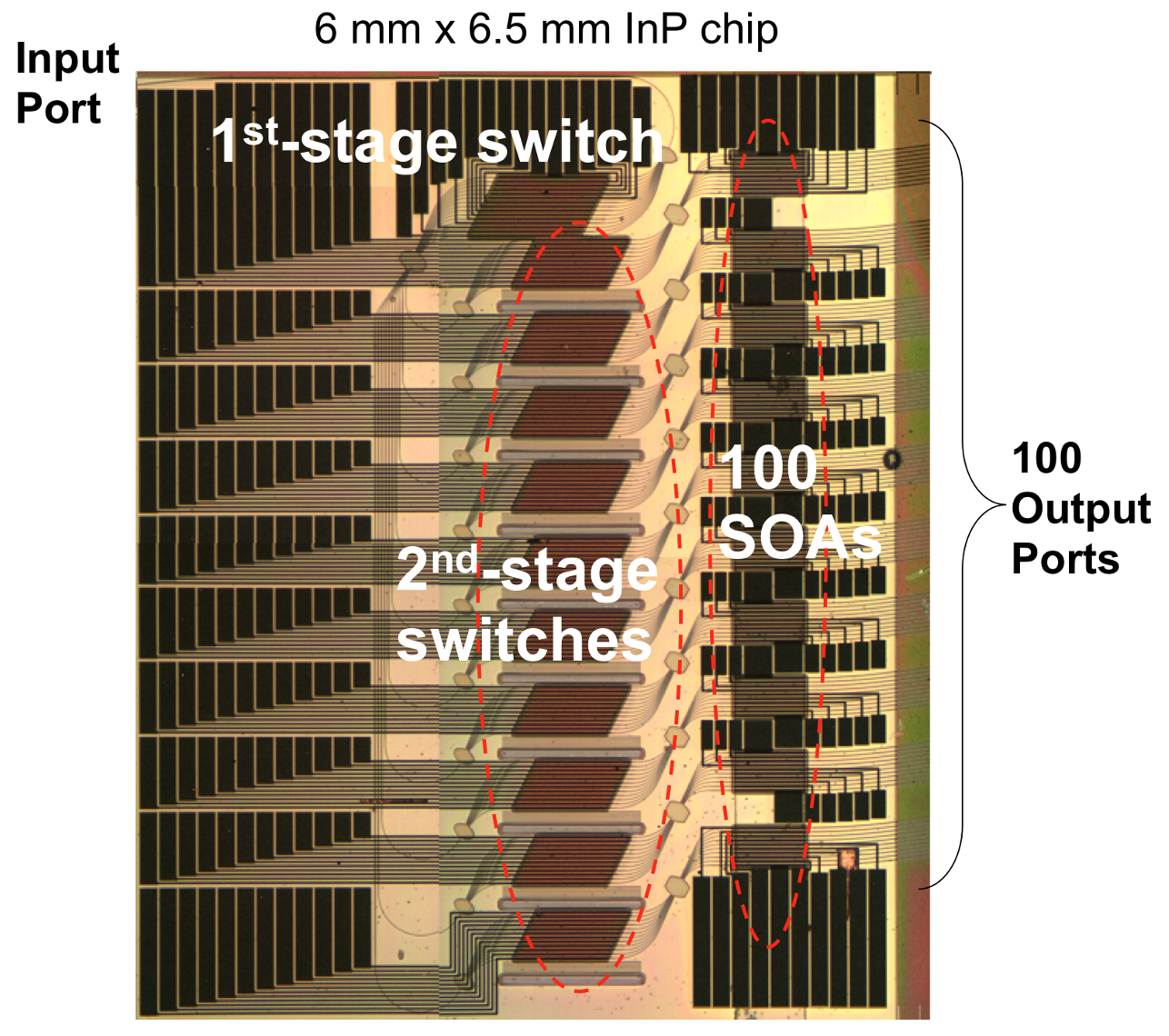 研究室サイトへ To the laboratory site中野 義昭 研究室 : 半導体光電子デバイスとそのプロセス技術の研究Yoshiaki Nakano Laboratory : Research on semiconductor optoelectronic devices and their processing technologies21世紀の光情報通信ネットワーク、光情報処理・記録に向けて、化合物半導体をベースにした新しい高性能な半導体レーザや半導体光制御デバイス(光スイッチ,波長変換器,光アンプなど)と、これらのデバイスを集積化して構成される高機能な半導体集積光デバイス・光集積回路を研究しています、またエネルギー問題の解決に向けて、化合物半導体に基づく新しい高効率な太陽電池の研究開発も行っています。2010年にスタートした総長直轄「太陽光を機軸とした持続可能グローバルエネルギーシステム」総括寄付講座の中核研究室です。これらデバイスを作製するための、InP、GaAs基板上の InGaAsP, InGaAlAs混晶などによる量子マイクロへテロ構造と、GaN、AlN、InN等のIII族窒化物量子マイクロヘテロ構造の結晶成長や加工技術も、研究対象です。Optoelectronic devices are studied, including semiconductor lasers, light emitting diodes, photovoltaic cells, optical switches, and photonic integrated circuits, as well as their applications to energy and information/communication systems. Main subjects of current research are as follows: (1) metal-organic vapor phase epitaxy (MOVPE) and micro/nano fabrication technologies for group III nitride, InP, and GaAs based compound semiconductor quantum structures, (2) large scale and fast matrix optical switches, (3) monolithic lightwave synthesizer photonic integrated circuits, (4) micro-opto-electro-mechanical systems (MOEMS), (5) optical interconnect, (6) photonic networking, (7) compound semiconductor high efficiency solar cells, (8) solar fuel, (9) sustainable energy system based on sunlight.
 -
 研究室サイトへ To the laboratory site大矢 忍 研究室 : オールエピタキシャル酸化物単結晶量子ヘテロ接合を用いた新機能スピンデバイスの開拓Shinobu Ohya Laboratory : Novel functional spin devices based on all-epitaxial oxide single-crystal quantum heterostructures我々のグループでは、独自のオゾンアシスト酸化物分子線エピタキシー装置を利用して、酸化物や金属などからなる強磁性体や半導体を組み合わせたオールエピタキシャル単結晶ヘテロ構造の開拓を進めています。このようにして得られた薄膜を用いて、量子スピンデバイスなどの実現を目指しています。特に酸化物2次元電子界面における大きなスピン軌道相互作用を利用したスピン流と電流の高効率変換技術や、単結晶ヘテロ構造の高い結晶性を生かした高効率のスピン依存伝導デバイスの実現を目指しています。次世代の高度情報化社会において不可欠な、不揮発かつ低消費電力の様々な新機能スピントロニクスデバイスの実現に向けた取り組みを進めています。We are developing all-epitaxial single-crystal heterostructures consisting of oxide/metal ferromagnets and semiconductors using our unique ozone-assisted oxide molecular-beam epitaxy technique. We aim to realize quantum spintronics devices using these thin films. In particular, we aim to realize highly efficient spin-charge current conversion by utilizing the large spin-orbit interaction at two-dimensional electron gas formed at oxide interfaces. In addition, we aim to develop spintronic devices using highly efficient spin-dependent transport in our heterostructures with high crystallinity. We are working to realize a variety of new functional non-volatile spintronics devices with low-power consumption, which will be indispensable in the next-generation advanced information society.
 -
 研究室サイトへ To the laboratory site種村 拓夫 研究室 : 半導体集積フォトニクスTakuo Tanemura Laboratory : Semiconductor integrated photonics数ミリ角の半導体チップの内部に光を閉じ込め、その状態を自在に操る技術を研究しています。「電子」にはない「光」ならではの特徴を活かしながら、頭の良い演算は「電子」回路に任せる、いわゆる“良いところ取り”の光電子集積チップを創出し、次世代光通信、光配線、イメージング、センシングなど、幅広い分野への応用を目指しています。研究分野は、大きく分けて、化合物半導体ナノフォトニックデバイス、大規模光集積回路(pLSI)、超高効率太陽電池、太陽光を機軸とする再生可能エネルギーシステムの4つです。We are researching technology to confine light inside a semiconductor chip of several millimeters square and to freely manipulate its state. While taking advantage of the unique characteristics of "light" that "electronics" do not have, we will create opto-electronic integrated chips that leave clever calculations to "electronic" circuits. We aim to apply it to a wide range of fields, such as imaging and sensing. Our research fields can be broadly divided into four areas: compound semiconductor nanophotonic devices, large-scale photonic integrated circuits (pLSI), ultra-high-efficiency solar cells, and renewable energy systems centered on sunlight.
 -
 研究室サイトへ To the laboratory siteドロネー ジャン ジャック 研究室 : センシングとエネルギー変換のための光デバイスJean-Jacques Delaunay Laboratory : Optical devices for sensing and energy conversion当研究室では、マイクロ/ナノ構造体の作製と、それを用いたエネルギー変換デバイスやサブ波長領域の光デバイスを専門としています。マイクロ・ナノ加工技術の高度化により、外部環境と強く相互作用するマイクロ・ナノ構造を設計・作製することができるようになりました。例えば、メソポーラス材料に空気中の水分子を効率よく吸着させれば冷却に利用できますし、金属構造中の光と物質の相互作用の強さを利用すれば、生物・医療用の高感度センサーや通信用の超高速全光スイッチの実現が可能です。Our group specializes in the fabrication of micro/nanostructures and their use in energy conversion devices and optical devices with sub-wavelength dimensions. By advancing micro/nanofabrication techniques, we are able to design and fabricate micro/nanostructures that interact strongly with their external environment. For example, efficient sorption of airborne water molecules on mesoporous materials can be used for cooling purposes, and enhanced light-matter interactions in metallic structures can be exploited to realize highly sensitive sensors for biological/medical applications or ultra-fast all-optical switches for telecommunications.
 -
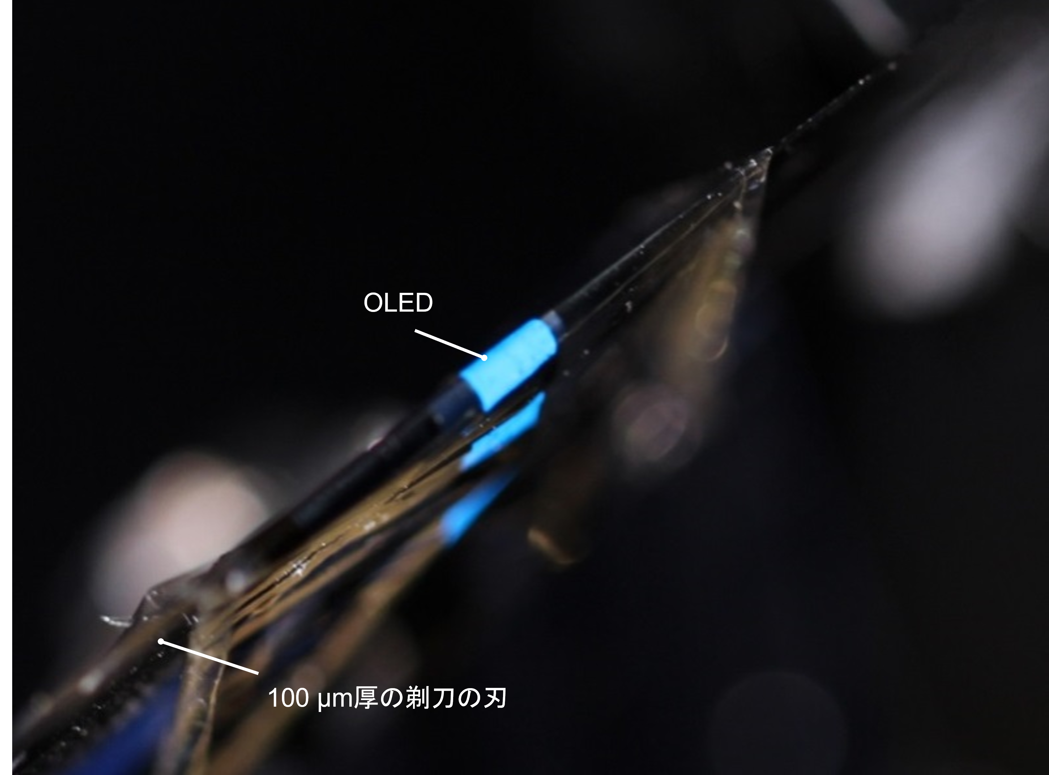 研究室サイトへ To the laboratory site横田 知之 研究室 : 有機エレクトロニクスのフレキシブルセンサ応用Tomoyuki Yokota Laboratory : Organic Electronics for flexible sensor application横田研究室では、有機半導体を用いた柔らかいエレクトロニクスの研究・開発を行っています。柔らかいエレクトロニクスは、従来のシリコンをはじめとしたエレクトロニクスとは異なり、柔軟な有機材料などを用いることで、曲げたり伸ばしたりすることが可能です。これまでの研究で、極薄の基板上にエレクトロニクスを作製することに成功し、肌に直接貼ることのできるセンサや、着るだけで生体情報をセンシングすることのできる服型のウェアラブルエレクトロニクスを開発しています。Yokota Laboratory is developing soft electronics using organic semiconductors. Soft electronics can realize the flexibility and stretchability due to the softness of the organic materials. We have succeeded in fabricating electronics on the ultra-thin substrates, which can be directly laminated to the skin and used as skin sensor. In addition, we are developing the textile based wearable electronics that can measure the biometric information by being worn.
 -
 研究室サイトへ To the laboratory site新井 史人 研究室 : バイオロボティクスFumihito Arai Laboratory : Bio-robotics次世代の知能システムに必要とされる機能要素及びシステム制御・統合に関する教育・研究を行っています。主に、MEMS(微小機械システム)とナノテクノロジーを基盤としたロボティクス・メカトロニクスに関する研究を推進しています。マイクロ・ナノ領域の物理化学現象を理解し、バイオミメティックな視点を取り入れた高度集積化・知能システムを実現します。新原理センサ・アクチュエータ、微細加工分子操作を行う三次元ナノマニピュレーション、生体組織や細胞操作を行う自律型マイクロロボット、医療・バイオシステムなどの研究を通じてマイクロ・ナノ科学を学び、小型集積化技術や知能システムのフロンティア技術を習得します。ミリ・マイクロ・ナノロボットシステムの学術研究で社会に貢献することを目指します。Research and education on functional units for the future intelligent systems from micro and nano-scale. System integration based on MEMS and nanotechnology. The system design is based on physical and chemical phenomena in micro and nano domain and bio-mimetic approach. Our objective is to improve the QOL (Quality of Life) by the application of robotics and micro-nano technologies to biomedicine.
 -
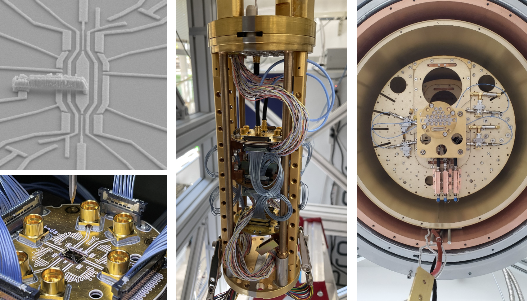 研究室サイトへ To the laboratory site山本 倫久 研究室 : 固体中の量子自由度の制御と伝送の技術に基づいた量子電子デバイスの創製Michihisa Yamamoto Laboratory: Creation of quantum electronic devices based on control and transmission technology of quantum degrees of freedom in solids本研究室では、固体中の量子自由度の制御と伝送の技術に基づいた量子電子デバイスの創製に取り組んでいます。具体的には、半導体微細構造中を伝搬する電子の量子状態を1電子単位で制御する量子電子光学実験や原子層物質における新たな量子自由度の伝送・制御の実験によって、量子コヒーレンスの広がりや量子相関、量子変換の物理を解明し、それに基づいた量子デバイスの指導原理を開発しています。同時に、高度な量子技術を用いて物性科学の問題をミクロな視点から解き明かし、量子技術と物性科学を融合させた新しいフロンティアを切り拓きます。Our laboratory is working on the creation of quantum electronic devices based on the control and transmission technology of quantum degrees of freedom in solids. Specifically, we are conducting quantum electron optics experiments that control the quantum state of electrons propagating in semiconductor microstructures on an electron-by-electron basis, and experiments on transmission and control of new quantum degrees of freedom in atomic layer materials. We are elucidating the physics of quantum correlations and quantum transformations, and developing guiding principles for quantum devices based on them. At the same time, we will use advanced quantum technology to solve problems in condensed matter science from a microscopic perspective, opening up new frontiers that fuse quantum technology and condensed matter science.
オープンイノベーション推進部門
-
 研究室サイトへ To the laboratory site塩見 淳一郎 研究室 : 分子から連続体へのマルチスケールな視点で熱エネルギー材料やシステムを開発Junichiro Shiomi Laboratory : Development of thermal energy materials and systems from a multi-scale perspective from molecules to continuum天然資源から得られるエネルギーの多くは利用されずに熱として排熱されていて、持続的社会の実現に向けてはこの排熱を他のエネルギー形態(電気など)に変換したり、蓄えたりして再利用する技術が重要です。私達のグループでは、分子から連続体へのマルチスケールな視点で材料を評価・デザインすることによって、熱エネルギーの有効利用へ貢献することを目指しています。また、同様の手法を用いて、界面を含む流体現象や、高分子複合材などの研究も行っています。Much of the energy obtained from natural resources is wasted as heat without being used, and in order to realize a sustainable society, it is necessary to convert this waste heat into other forms of energy (electricity, etc.) and store it. It is important to have a technology to re-use them. Our group aims to contribute to the effective utilization of thermal energy by evaluating and designing materials from a multi-scale perspective from molecules to continuum. In addition, using the same method, we are also researching fluid phenomena including interfaces and polymer composites.
 -
 研究室サイトへ To the laboratory site竹中 充 研究室 : シリコンフォトニクスで切り拓く次世代AI・IoTデバイスMitsuru Takenaka Laboratory : Next-generation AI/IoT devices pioneered by silicon photonicsシリコンを使って光電子集積回路を実現するシリコンフォトニクスの研究を進めています。GeやIII-V族化合物半導体、グラフェンなどの2次元材料をSiフォトニクスと組み合わせることで、光演算で深層学習を行うAI用プログラマブル光回路、光配線LSI、中赤外集積回路などの研究を進めており、ムーアの法則に依らない革新的コンピューティングの実現を目指しています。We are conducting research on silicon photonics to realize optoelectronic integrated circuits using silicon. By combining two-dimensional materials such as Ge, III-V compound semiconductors, and graphene with Si photonics, we are promoting research on programmable optical circuits for AI that perform deep learning using optical operations, optical interconnection LSIs, and mid-infrared integrated circuits. We aim to realize innovative computing that does not rely on Moore's Law.
新川崎サテライト部門
-
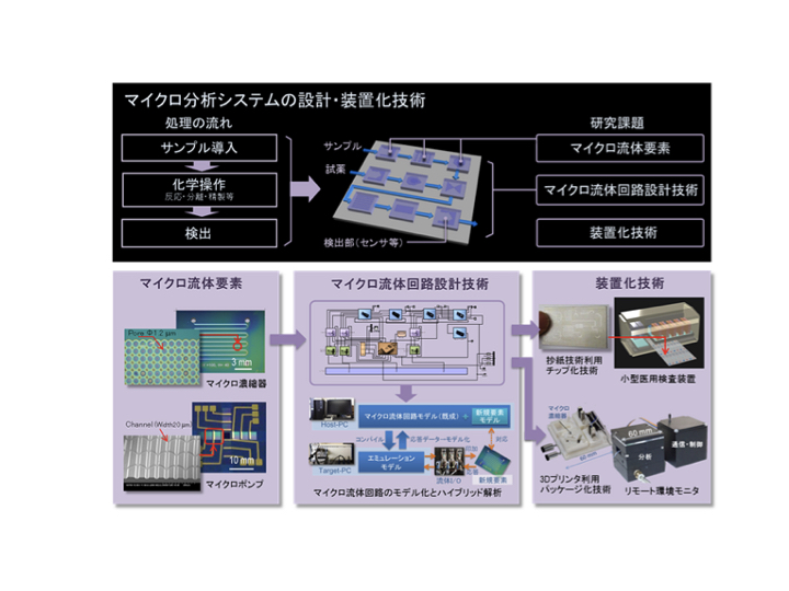 研究室サイトへ To the laboratory site三宅 亮 研究室 : マイクロ流体デバイス設計製作技術の開発Ryo Miyake Laboratory : Development of design and fabrication technologies for micro-fluidic devicesマイクロ流路や、マイクロミキサ、マイクロポンプなどのマイクロ流体要素のモデル化及びそれらを集積化したマイクロ流体システムの設計技術を開発・整備することで、バイオ・医療・環境向けのマイクロ分析システムや化学生産向けマイクロリアクタの集積化、装置化を加速・支援します。Integration and systemization of miniaturized bio-chemical analysis systems, micro-reactors based on design and fabrication technologies for micro-channel, micro-mixer, micro-pumps and their integrated circuits
 -
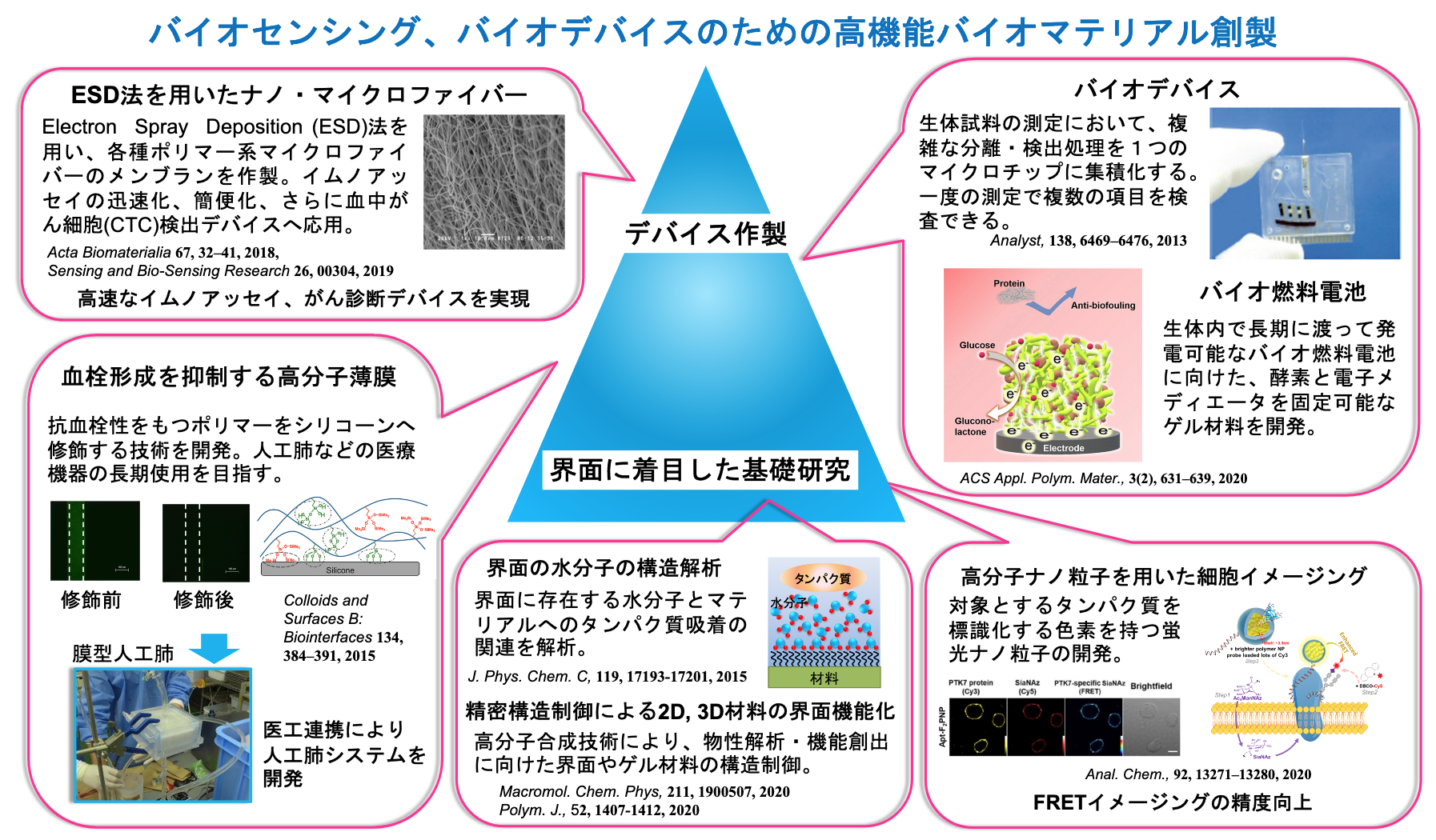 研究室サイトへ To the laboratory site高井 まどか 研究室 : 革新的医療を実現するための機能性マテリアル創製Madoka Takai Laboratory : Creation of functional materials to realize innovative medicine私たちの豊かで安心・健康な生活を実現するには、医療技術の進展、環境・エネルギーなどの地球規模の問題の解決、さらにエレクトロニクス技術の発展が基盤となります。そして、どの分野でも新しい機能性マテリアルの開発が必要不可欠です。私たちの研究室では、革新的医療を実現するための機能性マテリアル創製の研究をしています。医療分野で必要とされる新しい機能を確保するための設計概念は、第一に、人に優しいマテリアルであることです。生物は実に上手く生きるための機能を獲得しています。生物から学び、それをテクノロジーに活かして、人に優しい新しいバイオマテリアルの創製を目指します。自然界には機能発現のメカニズムがわかっていない不思議な現象がまだ数多くあります。特に、生命の最小単位である細胞や、タンパク質など生体高分子が機能を発現するには、水が関わっています。そのため、マテリアルと生体(バイオ分子)と水といった動きのある界面を、理解することが必要不可欠です。そこで機能性発現のメカニズムを、分子レベルで探求し解明し、新機能マテリアルの設計に活かし、新規マテリアル創製へ結びつけたいと考えています。また、研究室で得られた知識と技術を実際に社会で使ってもらえる製品として世の中に送り出すことも、工学分野で医療技術を研究する者の使命だと考えます。Advances in medical technology, the resolution of global issues such as the environment and energy, and the development of electronics technology are the foundations for realizing a prosperous, safe, and healthy life for us. And the development of new functional materials is essential in any field.In our laboratory, we are researching the creation of functional materials to realize innovative medicine. The design concept for securing the new functions required in the medical field is, first of all, human-friendly materials.Organisms have acquired functions to live really well. We aim to create new human-friendly biomaterials by learning from living organisms and applying them to technology. In the natural world, there are still many mysterious phenomena for which the mechanism of functional expression is unknown. In particular, water is involved in the functions of cells, which are the smallest unit of life, and biopolymers such as proteins.Therefore, it is essential to understand the dynamic interfaces between materials, living organisms (biomolecules), and water. Therefore, I would like to explore and clarify the mechanism of functional expression at the molecular level, apply it to the design of new functional materials, and connect it to the creation of new materials. In addition, I believe that it is the mission of those who research medical technology in the engineering field to send the knowledge and technology acquired in the laboratory out into the world as products that can actually be used in society.
 -
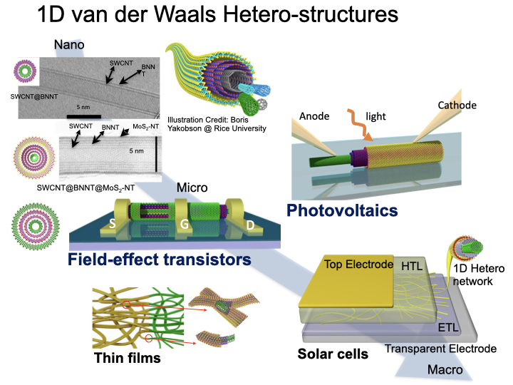 研究室サイトへ To the laboratory site丸山 茂夫 研究室 : 一次元ヘテロ構造の合成とデバイス展開Shigeo Maruyama Laboratory : Synthesis and device applications of one-dimensional heterostructures単層カーボンナノチューブ(CNT)をテンプレートとして,窒化ホウ素ナノチューブ(BNNT)や遷移金属ダイカルコゲナイドナノチューブ(TMD-NT)を同心状にファンデルワールス積層した一次元ヘテロナノ構造が形成できます。幾何学構造によって金属や様々なバンドギャップの半導体となるCNT、トンネル層となるBNNT、さらに遷移金属とカルコゲンの種類によって電子構造を制御できるTMD-NTを同心積層することで、直径が数ナノメートルでありながら様々なデバイス機能を持つナノ構造の創成が可能になります。このような一次元ヘテロ構造の原子スケールでの構造解析に加え、内層の半導体型CNTを主役とした電界効果効果トランジスタ、内層のCNTと外層のTMD-NT間のチューブ間励起子に着目した超微細光電変換デバイスなどへの応用を開拓しています。また、このヘテロ構造を用いた太陽電池など、マクロスケール応用も同時に展開しています。Using single-walled carbon nanotubes (CNTs) as templates, one-dimensional heterostructures can be formed through coaxial staking of boron nitride nanotubes (BNNTs) and transition metal dichalcogenide nanotubes (TMD-NTs). A wide variety of tunability of physical properties of CNTs and TMD-NTs that depend on the geometric structures and the combination of elements will open the way to fabricate novel nanostructures with various device functionalities. In addition to the atomic-scale structural analysis of such 1D heterostructures, we are working on nano-microscale device applications: e.g., field-effect transistors in which inner-layer semiconducting CNTs play a key role, and ultrasmall photovoltaic devices with a focus on intertube excitons formed between inner CNTs and outer TMD-NTs. We are also developing macroscale applications by applying 1D heterostructure thin films as active layers in solar cells.