At our center, we are updating the facilities and equipment in order to realize more advanced and fulfilling research.
新川崎サテライト部門
Shin-Kawasaki Satellite Division
NANOBICと4大学ナノ・マイクロファブリケーションコンソーシアム 新川崎・創造のもりに 2012 年4月にオープンしたナノ・マイクロ産学官共同研究施設「 NANOBIC ~ Global Nano Micro Technology Business Incubation Center」 川崎市は、慶應義塾大学、早稲田大学、東京工業大学、東京大学からなる「4大学ナノ・マイクロファブリケーションコンソーシアム」との連携により、ナノ・マイクロ分野の最先端の研究機器の共同利用や研究・教育などの支援に取り組み、川崎市内のものづくり企業の技術力と研究開発力の向上、産学連携による新産業の創出を目指しています。 N A N O B I C は 、ナ ノ・マ イクロ 技 術 に か か わ る 基 礎 研 究 か ら 試 作 、計測・評価まで一気通貫で取り組むことができるナノ・マイクロ技術の産学官共同研究開発拠点です。
クリーンルームの総面積379m2あり、クラス10000(206m2)のホワイトルームとクラス100(173m2)のイエロールームに分かれています。
Nano/Micro Fabrication Consortium with 4 Universities Nano/Micro Fabrication Consortium “NANOBIC ~ Global Nano Micro Technology Business Incubation Center” opened in April 2012 in Shin-Kawasaki Sozo no Mori. Through collaboration with the "Four Universities Nano/Micro Fabrication Consortium" consisting of Waseda University, Tokyo Institute of Technology, and the University of Tokyo, we are working to support joint use of cutting-edge research equipment in the nano/micro field and research and education. We aim to improve the technological capabilities and research and development capabilities of manufacturing companies in the city, and to create new industries through industry-academia collaboration. NANOBIC is an industry-university-government joint research and development base for nano/micro technology, which can handle everything from basic research related to nano/micro technology to prototyping, measurement, and evaluation.
The clean room has a total area of 379m2, divided into a class 10000 (206m2) white room and a class 100 (173m2) yellow room.
Area : 206m2
Cleanliness: Class 10000
(No more than 10,000 particles with a size of 0.5 μm or larger contained in 1 cubic foot (approximately 30 cm square) of air)
Area : 173m2
Cleanliness: Class 100
(100 or less particles with a size of 0.5 μm or larger contained in 1 cubic foot (approximately 30 cm square) of air)
Please feel free to contact us for anything related to microfabrication and evaluation. Our technical staff will work with you to come up with a solution. It's free.
All users are required to attend safety training. After completing the safety course, an ID will be issued and you will be able to reserve the equipment.
Reserve the device to be used from the reservation system website. (ID and PW are required) Coordinators and staff can act on your behalf for the first time.
Users are free to operate. If you are using the equipment for the first time, our technical staff will give you a detailed explanation. In principle, we do not accept outsourced processing or work on behalf of our technical staff.
06
支払い請求
payment request
利用料は月末締めで集計し、請求先様に連絡いたします。 内容を確認後、指定口座にお振込みください。
The usage fee will be totaled at the end of the month and will be sent to the billing address. After confirming the contents, please transfer to the designated account.
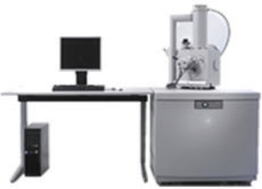
Atmosphere-controlled scanning electron microscope
Quanta 250/EDS
Manufactured by: FEI Japan Ltd.
Main applications/features.
-Water content control (wet observation), high temperature heating observation, high vacuum SEM observation
Main functions and options
Electron gun: tungsten
Resolution: 3.0 nm (high vacuum: high acceleration voltage 30 kV)
8.0 nm (low vacuum: low acceleration voltage 3 kV)
3.0 nm (ESEM)
Sample chamber vacuum: 6 × 10⁻⁴ Pa (high vacuum)
10 to 130 Pa (low vacuum)
10 to 2600 Pa (ESEM)
Accelerating voltage: 0.2 to 30 kV
Irradiation current: max. 2 mA
Magnification: x6 to 1,000,000
Sample exchange: draw-out system
Sample size: max. ø 100 mm, H 50 mm
Detector: secondary electron detector: ETD (scintillator type) (high vacuum)
LF-GSED (wide-field type) (low vacuum)
GSE type (ultra-low vacuum)
Semiconductor reflection electron detector
Accessory equipment: infrared CCD camera, heating stage (up to 1000°C), cooling stage (-20 to +60°C)
EDS (Oxford Instruments Ltd) INCA Energy250 x-act
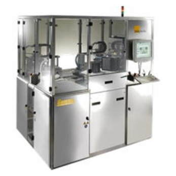
Manufactured by: Shibaura Mechatronics Co.
Main applications and features
Load-lock type sputtering equipment
Equipped with a sputtering source with good distribution over a wide area
Main Functions and Options
Sputtering method: Side sputtering
Sputter source: φ76 mm × 4
Substrate holder size: φ220 mm, in-plane film thickness variation within ±5% φ170 mm (SiO2)
Achievable pressure: 5 × 10⁻⁴ Pa or less
Exhaust time: 7 × 10⁻³ Pa or less in 10 minutes
Heating temperature: 300°C max.
Target: ITO, Ti, SiO2, AZO, Ni, Al, TiO2, Cr, Ag, Si, Sn, Au, Pt, Ni-Cr, Ti-Ni, Cu, etc.
(Please inquire about targets)
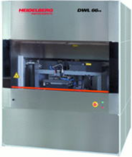
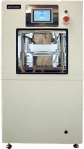
Manufacture: Heiderberg Instruments Mikrotechnik
Main applications/features.
Photomask production, direct writing
Main features and options
Electron gun: ZrO/W thermal field emission type
Accelerating voltage: 80 kV, 50 kV, 25 kV
Light source: Ar ion laser Wavelength: 363 nm, output: 180 mW
Maximum substrate size: 9 in. x 9 in.
Maximum writing size: 200 x 200 mm
Minimum writing size: 1.0 µm
Minimum address grid: 10 nm
Writing speed: 29 - 416 mm2/min
3D exposure mode
Camera system for alignment
Data formats: DXF (recommended), GDSll (recommended), CIF, Gerber, BMP, Ascii, STL
Grayscale exposure supported
Manufactured by: Zuse Microtech Ltd.
Main applications/features.
Fully automatic process for spin-coating, spray-coating, developing, baking and vapour priming of photoresist.
High uniformity and reproducibility.
Continuous processing of up to 25-50 wafers.
Main features and options
Compatible substrate sizes: 2, 3 and 4 inch, some odd-shaped substrates can also be handled.
Wafer handling: fully automatic, recipes can be created.
Can also be used for applying resist brought in from the factory.
Bakeable temperature range: 60-250°C
Spin-coating uniformity: within ±1.0% (at 10 µm film thickness)
Installed resists: OFPR 800LB 23cp, AZP4620
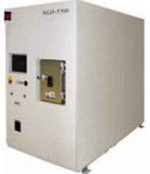
Manufactured by ULVAC Co.
Main applications/features
Dry etching of quartz, etc.
Dry etching equipment with low pressure, low electron temperature and high density plasma by magnetic neutral beam plasma (NLD).
Dry etching equipment with low pressure, low electron temperature and high density plasma by magnetic neutral beam plasma (NLD)
Dry etching equipment with low-pressure, low-electron temperature and high-density plasma using magnetic neutral beam plasma (NLD).
Etching with excellent shape and surface smoothness is possible.
Thick film resist can be used as a mask for deep etching (100 µm or more) of quartz and glass.
Thick film resist can be used as a mask for deep etching (100 μm or more) of quartz and glass
High-speed etching is possible (quartz > 1 μm/min, Pyrex > 0.8 μm/min).
Main functions and options
Plasma source: magnetic neutral beam plasma (NLD)
Substrate size: ø 150 mm
Substrate stage: mechanical chuck, chiller temperature control (-20 to 40 °C), He cooling mechanism
RF power supply: antenna: 2 kW (13.56 MHz), bias: 600 W (12.5 MHz)
Exhaust system: etching chamber: TMP (2800 L/sec) + DRP
Gas introduction system: CHF3, C3F8, SF6, O2, Ar, N2, He
Applications: Quartz only, other than quartz, please consult.
Other : Load lock chamber
〒212-0032
7-7 Shin-Kawasaki, Saiwai Ward, Kawasaki City, Kanagawa Prefecture
Shin-Kawasaki Sozo no Mori Area KBIC/ NANOBIC/ AIRBIC
Reception place for equipment use: AIRBIC Room A34
By train
10-minute walk from Shin-Kawasaki Station on the JR Yokosuka Line
15-minute walk from Kashimada Station on the JR Nambu Line
for automobiles
From Fuchu Highway (National Route 409), turn left at Shimohirama Intersection, 1km from JR Shin-Kawasaki Station, cross the Kashimada overpass and turn left for 600m.
Turn right at the Minamikase intersection from the Shitte Kurokawa Road (for Daini Keihin/Kawasaki), turn left at the T-junction under the Kokura overpass, and drive 250m.
Paid parking available