In the Device Prototyping Development Division, a variety of ultrafine processing equipment can be used, centered on the clean room of the Takeda Building (Asano Campus).
The Takeda Advanced Science Building was completed in December 2003. It is located in the southern part of Asano Campus. It was built by a donation from Ikuo Takeda, the founder of Takeda Riken Kogyo Co., Ltd. (currently Advantest Co., Ltd.).
The Takeda Building is the first University of Tokyo building to be named after an individual.
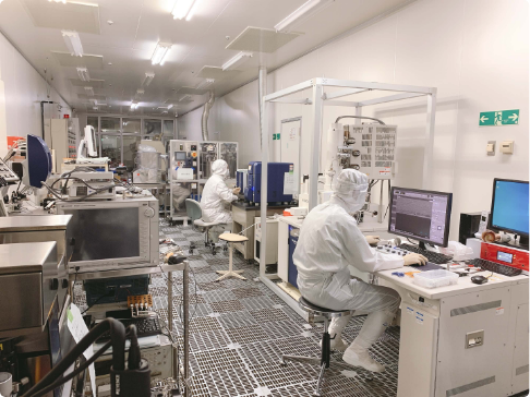
There is a super clean room on the second basement floor of the Takeda Building, where you can use various devices.
There is a large-scale clean room facility with a total area of 600m2 on the second basement floor of the Takeda Advanced Science Building.
It is divided into three rooms with different levels of cleanliness, and work can be carried out according to each level of cleanliness.
Available from inside and outside the university.
Area : 155m2
Cleanliness: Class 1
(No more than 1 particle with a size of 0.5 μm or larger contained in 1 cubic foot (approximately 30 cm square) of air)
Main work : Lithography, Exposure, Rendering
Area : 300m2
Cleanliness: Class 100
(100 or less particles with a size of 0.5 μm or larger contained in 1 cubic foot (approximately 30 cm square) of air)
Main work : Deposition, film processing, etching
Area : 145m2
Cleanliness: Class 1000
(No more than 1000 particles with a size of 0.5 μm or larger contained in 1 cubic foot (approximately 30 cm square) of air)
Main work : Morphology/Shape observation/Analysis/Electrical measurement/Cutting/Polishing/Joining
First of all, please feel free to contact us by e-mail from the inquiry page.
A team of playing managers and skilled research assistants with a wealth of practical experience in companies, Europe, and the United States will be available for consultation.
We will provide face-to-face technical consultation. Please explain and confirm the following points.
- Purpose of use (Commercial use is not accepted.)
- About Nanotechnology Platform
- Operation policy of this site
- Selection of usage form, specific support, assignment of person in charge, etc.
03
申し込み
application
利用申込書を技術相談の後にお渡しいたしますので、ご記入の上提出願います。
After the technical consultation, we will send you an application form, so please fill it out and submit it.
In order to use it independently, it is necessary to take a clean room class (held once a month) or a refresher and newcomer class (held every May). If you handle chemical substances, you will be asked to attend an environmental safety seminar and tour.
If there is a person qualified to enter the room or a support staff attends (for a fee), you can enter the room immediately and use the equipment. With the exception of some devices, reservations are made from a PC. After use, self-report the amount of use to the log system from the iPod or PC in the clean room. You will receive a billing statement by e-mail, so please reply after checking the contents. An invoice will be sent.
Please submit one A4 usage report. Submission is required because we have been able to realize inexpensive fees with the support of the Ministry of Education, Culture, Sports, Science and Technology. For non-submission, the fee will be approximately three times that for publication.
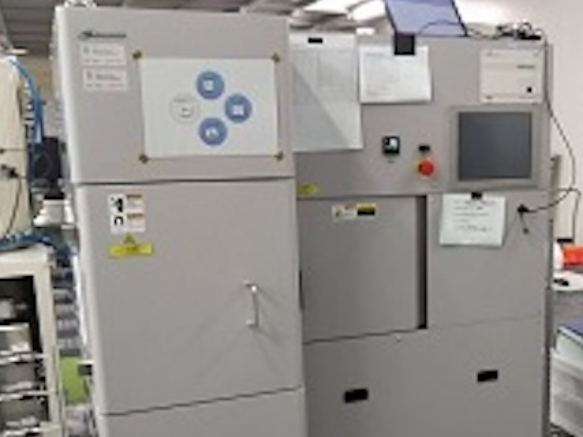
Manufactured by Shibaura
[Model No.] Shibaura CFS-4EP-LL i-Miller
[Functions] Vacuuming is fast and
sputtering can usually be started in about 10 minutes.
Stable film quality can also be expected.
Load lock type.
Standard equipped with a sputtering source
with good distribution over a wide area.
Compatible with a wide range of deposition materials
Targets are common to CFS-4ES.
Pt/Au/Cr/Ti are fitted as default.
Other targets are exchanged with the technical assistance
of support staff.
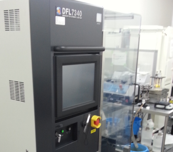
Manufactured by DISCO
[English] Silicon Stealth Dicing Machine
Stealth Dicing Machine
[Model Number] DISCO DFL7340 (Stealth Dicer for Si)
The stealth dicer at this location is exclusively for silicon,
but it is a dicer that uses a new technology from Japan called 'stealth dicing technology'.
(By focusing a laser beam inside a silicon wafer,
it is possible to intentionally embed "breakable lines".
By embedding a number of these lines according to the blueprint,
and then lightly stressing the wafer at the end,
the dicer is a dream dicing machine that can cleave the wafer according to the blueprint.
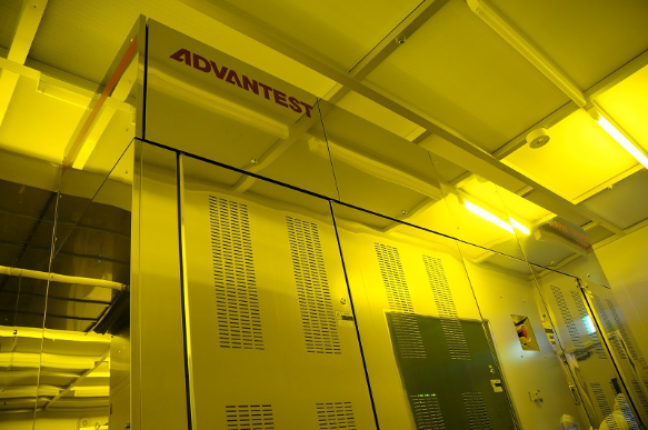
Ultra-high-speed, large-screen stacked wire drawing system F-7000
Patterning
EB exposure system
Manufactured by Advantest
The F7000 is an EB lithography system that uses an electron beam to write patterns at the 1Xnm node. It can write on substrates of various materials, sizes and shapes, including wafers and templates for nanoimprinting, and supports diverse applications such as advanced LSI, photonics, MEMS and nanofabrication.
The column, which is the key to electron beam writing accuracy, has been newly developed to achieve the resolution performance required at the 1Xnm node, which is essential for research and development of cutting-edge devices.
Capable of writing on substrates of various sizes, shapes and materials
The adjuster mechanism enables imaging on wafers of various sizes and square-shaped substrates such as glass substrates. By replacing the adjuster, substrates made of different materials, such as silicon and gallium arsenide, can be handled by the same machine without causing contamination.
Resolution: 1Xnm.
Substrates to be exposed: wafers (300 mm, 200 mm, 6~3 in), glass substrates (6025).
Exposure method: CP exposure method, VSB exposure method
The F7000 series is a system that uses an electron beam to directly lithograph circuit patterns on silicon wafers, etc. It can be used for research and development of advanced semiconductors for 1Xnm node miniaturisation, and can lithograph at industry-leading processing speeds (5 times faster than the F3000, which supports 65nm nodes). ). The self-cleaning mechanism and adjuster function ensure stable operation over long periods of time, and the system is also capable of writing on substrates other than silicon wafers.
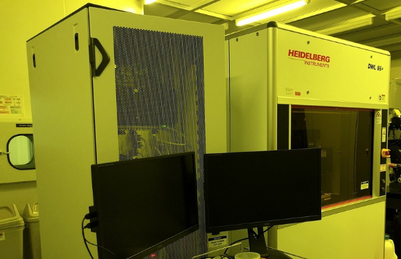
Manufactured by Heiderberg Instruments Mikrotechnik
[Model Number] HEIDELBERG DWL66+
[Function] 406nm wavelength with small piece alignment option and double-sided alignment function. The 1024-gradation 'greyscale lithography' allows a certain degree of freedom in creating three-dimensional shape steps in the photoresist. In addition, the GenISys conversion software 'BEAMER' calculates the influence of proximity effects and compensates for exposure in order to obtain the shape.
The DWL 66+ is a high-resolution direct laser lithography system suitable for research and development applications and for small lot production, mask creation and maskless exposure.
It is equipped as a standard system with all the functions required for the production and analysis of microstructures.
Due to its high throughput and the wide range of applications it can be used for, e.g. MEMS and micro-optics.
The system contributes to the research and development of applications requiring microstructure fabrication.
Features.
For maskless exposure and mask creation.
2.5D grayscale exposure mode (standard 128 shades, optional 255 or 1000 shades)
Abundant functions and expandability for multiple applications
Switchable between 6 drawing modes (0.3um-4.0um) (pixel size).
High-precision overlay with backside alignment possible
Maximum substrate size of 9" x 9" supported
Supports a wide range of data formats
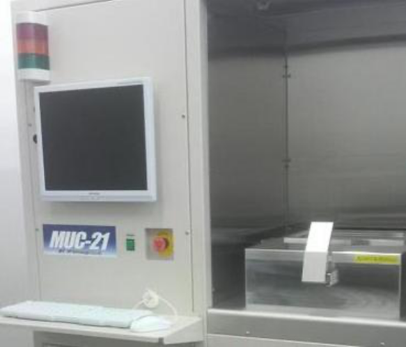
Ultra Rapid Silicon Deep Reactive Ion Etching Machine
Manufactured by Sumitomo Precision Industries, Ltd.
[Model Number] SPTS MUC-21 ASE-Pegasus
[Functions] High-density plasma (ICP power up to 3kW, 1800W normal use) enables low-damage, high-speed etching.
100 nm class aperture special recipe available. Also available are recipes that can be conveniently used in combination, such as 'dry release' with SF6 and oxide film etching with C4F8.
High etch rate processing
High mask selection ratio processing
High aspect ratio processing
Hardware modules and
Process software included
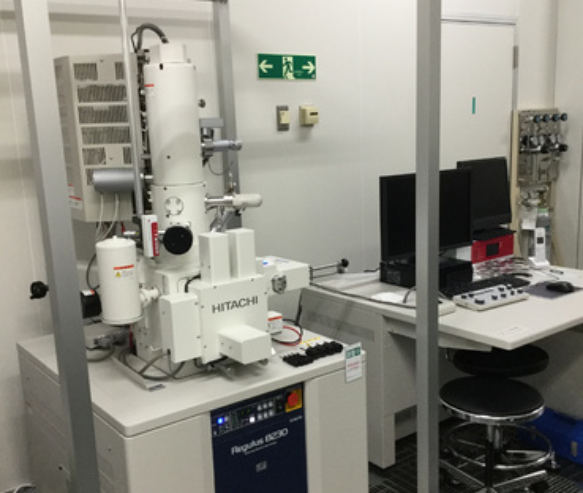
Ultra-high Resolution Scanning Electron Microscope
Manufactured by Hitachi High-Tech
Field Emission Scanning Electron Microscope
Ultra-high Resolution Scanning Electron Microscope
FE-SEM Hitachi Regulus 8230
[Model Number] HITACHI Regulus 8230
Equipped with a cold FE electron gun that is most suitable for high-resolution observation with low aberration and low acceleration voltage.
Resolution improved by approximately 20% compared to conventional models.
(Regulus8220/8230/8240: 0.9 nm/1 kV, Regulus8100: 1.1 nm/1 kV)
Maximum magnification extended from 1 million times to 2 million times (Regulus8220/8230/8240)
User support functions to fully demonstrate high performance
SEM signal detection status display function as one of the user support functions
Displays the operating principle of the detector used and the signals obtained, supporting observations with a variety of detection systems.
〒113-0032
2-11-16 Yayoi, Bunkyo-ku, Tokyo
When coming to the University of Tokyo Takeda Science Building, the following two stations are convenient.
Subway Chiyoda Line Nezu Station (C14) 5 minute walk from Exit 1
Subway Namboku Line 10 minute walk from Todaimae Station (N12) Exit 1 Located on the Asano Campus.
(Please be careful not to confuse it with the Yayoi Campus.